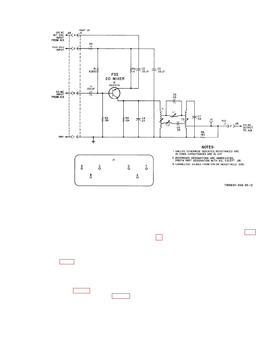
 |
|||
|
|
|||
|
|
|||
| ||||||||||
|
|  output termination and minimizes
be varying. The signal from A10 is genera-
variations due to discriminator
ted by a crystal-controlled oscillator; this
loading. The combination of resis-.
signal is the reference frequency. The dc
tor R9 and capacitor C11 prevents
output voltage, proportional to the phase
rf leakage into the +10-volt dc sup-
difference, is the automatic phase control
ply.
(ape) voltage applied to vfo module A9 (para
(3) The rf output of module A18 can be
measured at test jack J2.
voltage will assume a reference level to
maintain the vfo output frequency. If a
phase difference is detected, an error volt-
age is developed in the phase comparator.
This change in apc voltage opposes any
change in vfo output frequency by returning
Phase comparator module A17 contains
the vfo output to its correct frequency, and
phase comparator driver Q1 and the phase
establishes a phase lock.
comparator. The phase comparator com-
a. Phase Comparator Driver. The input
pares the phase of the signals from f ss if.
from fss if. module A18 is coupled through
module A18 (para 27) with those from in-
capacitor Cl to the base of phase com-
terval oscillator module Al0 (para 24). The
parator driver Q1. The amplified signal is
input signal from A18 is initially generated
by the vfo; the frequency of this signal may
coupled to the phase comparator by
|
|
Privacy Statement - Press Release - Copyright Information. - Contact Us |