 |
|||
|
|
|||
|
Page Title:
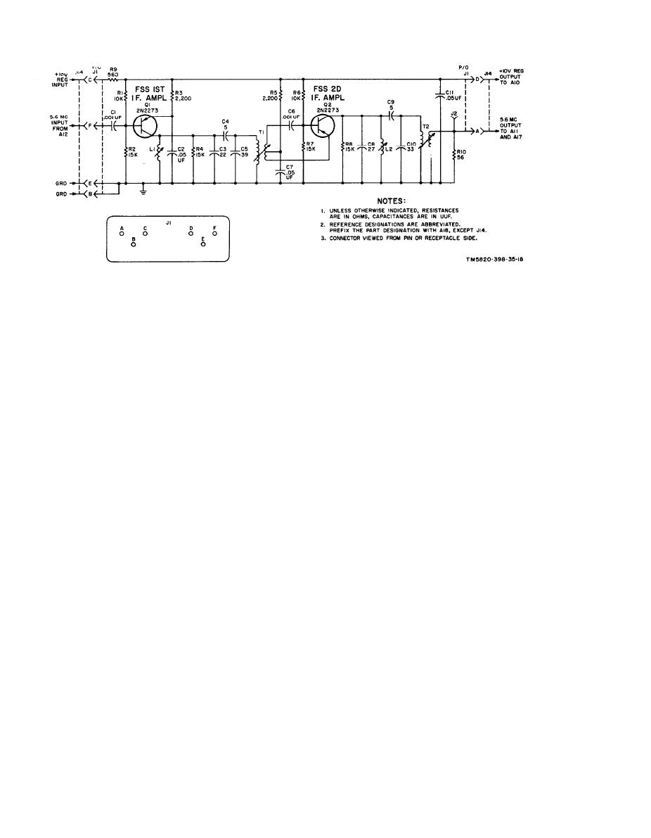
Figure 22. Speech amplifier limiter module A18, schematic diagram. |
|
||
| ||||||||||
|
|  transformer T1. Resistors R1 and R2 form
CR1, and E2 to CR2. (The E desig-
a voltage divider which provides the fixed-
nations are for purposes of refer-
bias portion of the emitter-to-base bias.
ence only.)
Emitter resistor R3 establishes the fixed
(2) The phase comparator also re-
ceives an input signal from crys -
portion of the emitter-to-base bias and
tal-controlled interval oscillator
stabilizes the emitter current. Capacitor
module A10 which is injected at the
C2 is a bypass capacitor for the Q1
center tap of transformer T1 and
emitter. Capacitors C5 and C6 and in-
ductor L1 form a pi-filter which prevents
the junction of diodes CR1 and CR2.
any rf signals from entering the 10-volt
This signal voltage (E3) is exactly
dc Supply
90 out-of-phase with voltages E1
and E2 when the frequency of the
5.6-mc input, developed initially by
parator consists of the tapped secondary
the vfo, is the same as the crystal-
winding of T1, coupling capacitors C3 and
controlled input frequency. This
C4, diodes CR1 and CR2, and resistors R4
condition exists when the vfo is on
and R5. The output voltage of the phase
frequency. When the two input sig-
comparator depends on the phase relation-
nals are 90 out-of-phase, the dc
ship of the two signals applied to the cir-
output voltage, which is the vecto-
cuit. The voltage output is pivoted about a
rial sum of voltages E1 plus E3 and
+3.5-volt dc reference level at the junction
E2 plus E3, will be at the +3.5-volt
of resistors R6 and R7 which is applied to
reference level.
the center tap of transformer T1 and,
(3) Diode CR1 receives a voltage equal
through the secondary winding of trans-
to the sum of El and E3; diode CR2
former T3 in module A10, to the junction
receives a voltage equal to the sum
of diodes CR1 and CR2. This voltage is
of E2 and E3. The diodes rectify the
established by the divider action of resis-
signals, and dc voltages appear
tors R6 and R7 which are connected across
across load resistors R4 and R5.
the 10-volt power supply. Capacitor C7 is
an rf bypass capacitor.
When the signal voltages are equal,
the output voltages across resis-
(1) The signal induced in the secondary
tors R4 and R5 are equal, and the
of T1 is coupled through capacitors
total voltage across both resistors,
C3 and C4 to diodes CR1 and CR2,
in respect to the junction of resis-
respectively, producing equal and
tors R4 and R5, is canceled out,
opposite voltages. E1 is applied to
34
|
|
Privacy Statement - Press Release - Copyright Information. - Contact Us |
