 |
|||
|
|
|||
|
Page Title:
Figure 4-5. Frequency Synthesizer Transmit-Receive Switch, Simplified Schematic Diagram |
|
||
| ||||||||||
|
|  TO 31R2-2GRC171-2
TM 11-5820-815-14
NAVELEX 0967-LP-544-5010
proximately 29 milliamperes. For the other two stages,
resistor R8 sets the collector current of Q4 at
the power splitter which separates the vco signal into two
approximately 29 milliamperes, and resistor R12 sets the
signal paths. One signal path feeds output amplifier
collector current of Q6 at approximately 51 milliamperes.
circuit A2A6 through -12-dB pad A2A4R12-R13-R14.
In the rf path, variable capacitor C1, variable capacitor
The other signal path feeds the regenerative divider
C5 in series with inductor L3, and variable capacitor C8
circuit of the variable divider through -15-dB pad
in parallel with inductor L4 allow adjustment of the 3-
A2A4R11-A2A7R21-R22-R23. Besides separating the
stage rf amplifier for maximum flatness over the
vco signal, the power splitter provides isolation between
frequency range of the synthesizer. In the base circuit of
the half frequency of the regenerative divider and vco
Q2. capacitor C23 compensates for lead inductance of
signal being fed to power amplifier circuit A2A6.
Q2. In the t12-V dc circuit, inductors L10, L5, andL2and
capacitors C11, C7, and C4 form a decoupling network
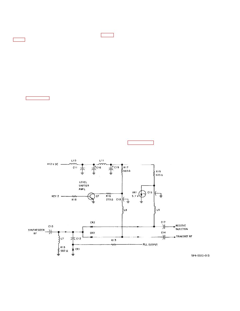
4-73. OUTPUT AMPLIFIER A2A6. Reference desig-
to decouple the rf amplifier from the +12-V dc line. At the
nators apply to output amplifier A2A6, Output amplifier
output of rf amplifier Q6, the signal is coupled through
A2A6 (figure FO-19) consists of a 3-stage rf amplifier (rf
C10 to the transmit/receive switch and is loosely coupled
amplifiers Q2, Q4, andQ6 and associated bias amplifiers
through capacitor C12 to detector diode CR1. The dc
Q1, Q3, and Q5) followed by a diode type (CR2 and
voltage developed across CR1 is brought out to the pll
CR3) transmit/receive switch. In the 3-stage rf amplifier,
output (testpoint 4 on chassis A10) to give an indication
bias amplifiers Q1, Q3, and Q5 set the collector currents
as to the level of rf at the input to the transmit/receive
of Q2, Q4, and Q6 respectively. Since all bias amplifiers
switch.
function the same, only bias amplifier Q1 will be
discussed. The voltage divider R2-R3 sets the base
4-74. TRANSMIT/RECEIVE SWITCH.
Reference
voltage of Q1 at about 9.4 V dc which fixes the emitter
designators apply to A2A6. The transmit/receive switch
voltage at about 10.0 V dc. The resulting voltage drop
(about 2 V dc) across R4 sets the collector current of Q1
output of the synthesizer or the receive injection output.
at ap-
In transmit mode, a logic 0 key 2
Figure 4-5. Frequency Synthesizer Transmit-Receive Switch, Simplified Schematic Diagram
4-17
|
|
Privacy Statement - Press Release - Copyright Information. - Contact Us |
