 |
|||
|
|
|||
|
Page Title:
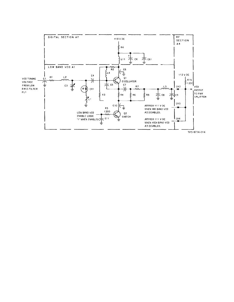
Figure 4-4. Voltage-Controlled Oscillator . Simplified Schematic Diagram |
|
||
| ||||||||||
|
|  TO 31R2-2GRC171-2
TM 11-5820-815-14
NAVELEX 0967-LP-544-5010
Figure 4-4. Voltage-Controlled Oscillator . Simplified Schematic Diagram
three bands. The only other difference is that the low-
band vco has a low-pass filter (A2A1L3, C8, and C9) at
in conjunction with capacitors A2A1C4 and A2A1C5,
its output to filter second harmonic frequencies which fall
determines the oscillating frequency of the vco. Tuning
below the 400-MHz upper frequency limit of the
voltage from low-pass filter A2A5FL1 applied through
synthesizer. Each vco is a sealed, non repairable,
resistor A2A1R1 and choke A2A1L2 to varactor
nonadjustable unit.
However, to understand circuit
A2AlCR1 causes the frequency of the vco to vary. As the
operation the low-band vco will be discussed.
tuning voltage increases, the capacitance of A2A1CR1
decreases causing the frequency to increase.
By
adjusting A2A1L1 and A2A1C3, the range of the vco
4-70. Radio control frequencies that fall in the low- band
frequency is set so varactor A2A1CR1 controls the
range cause the low-band decoder to apply a logic 1
voltage through resistors A2A7R18 and A2A1R5 to the
above the highest frequency (250 MHz) of the low band.
base of transistor switch A2A1Q2 turning it on. When on,
The vco output signal is developed across emitter
A2A1Q2 applies a ground to the voltage- controlled
resistor A2A1R4 and fed through coupling capacitor
oscillator circuit exciting A2A1Q1 into oscillation. At the
A2A1C7. resistive pad A2A1R6-R7-R8, low-pass filter
same time A2A1Q2 provides a current path to ground
A2A1C8-L3-C9, and diode A2A4CR2 to the vco output.
from the +12-V dc supply through A2A4R15, A2A4CR2,
Resistor values of A2A1R6, R7, and R8 are test selected
A2A1L3, and resistive pad A2A1R6-R7-R8. This forward
to set the output of the vco to about 800 millivolts which,
biases diode A2A4CR2 to enable the low-band vco
in turn, sets the synthesizer transmit rf and receive
output and at the same time reverse biases diodes
injection output levels at 14 2 dB mW when loaded into
A2A4CR3 and A2A4CR4 to open the midband and high-
50 ohms.
band outputs. In the vco circuit, voltage developed
across resistor A2A1R3 of voltage divider A2A1R2-
4-71.
Decoupling network A2A7R4-C61-C4-L1 de-
A2AlR3 and applied through choke A2A1L4 sets the bias
point of A2A1Q1. The tuned circuit, composed of
couples the three voltage-controlled oscillators from the
capacitor A2A1C3, varactor A2AlCRl, and inductor
+18-V dc supply voltage. This prevents the 3.2- MHz
A2A1L1
tcxo frequency from interfering with the vco frequency.
4-16
|
|
Privacy Statement - Press Release - Copyright Information. - Contact Us |
