 |
|||
|
|
|||
|
Page Title:
Variable 1 frequency divider 1A14A4 block diagram description |
|
||
| ||||||||||
|
|  TM 11-5820-695-35
becomes set. When flip-flop Z5 is set, the initialize
pulse (537 + 1 count) is applied to all the registers in
1A14A4 and 1A14A5 which sets the registers to a count
which enables the registers to be modified by the
thumbwheel switch setting. The initialize pulse also
prevents an additional count from being accumulated by
the 1.0 MHz register.
(b)
The next clock pulse following the
initialized condition is not counted by the registers but
sets flip-flop Z7. When flip-flop Z7 is set, the initialize
condition is terminated and an inhibit level is produced
(537 + 2 count) and applied to all registers. The next
(3) Variable 1 frequency divider 1A14A4 block
clock pulse resets flip-flop Z5 but is inhibited to the
registers. When flip-flop Z5 is reset, a preload pulse
set for 5000 MHz, the if output signal of 23.5655 MHz
(537 + 3 count) is generated and applied to the register
from 1A14A2 is applied to board A1 on variable 1
switch gates Z4, Z9 and Z16 on board Z2 causing the
switch gates Z4, Z9 and Z16 to open (540 count). With
CR1 and applied to the divide-by-2 circuit Z1 through
the switch gates Z4, Z9 and Z16 opened, the
driver Q1. The divided pulses are inverted through
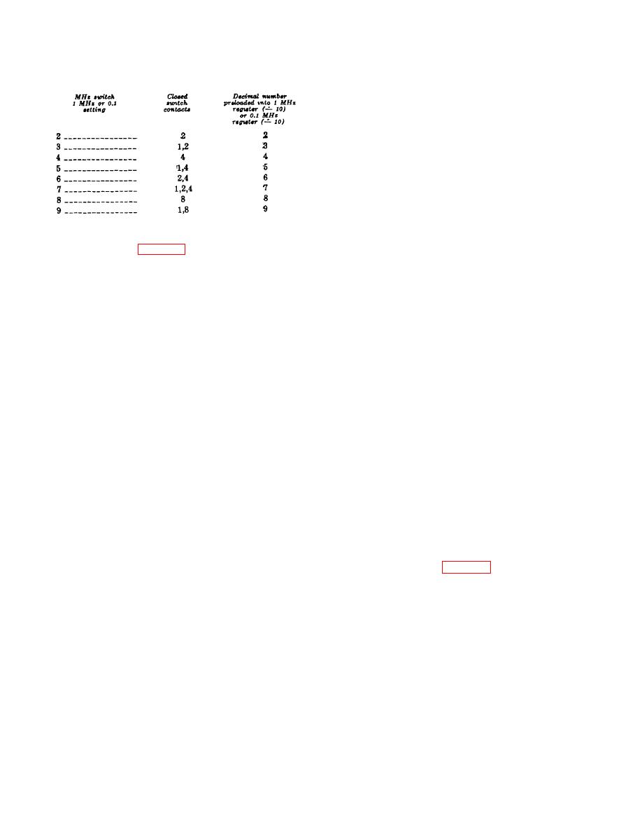
thumbwheel switch settings modify the count in the
input inverter Z2 and are the clock pulses for operating
registers.
both the first stage of the 0.1 MHz divide-by-10 register
and the control flip-flops Z5 and Z7. The countdown
(c)
The next clock pulse is applied to the
cycle begins when all stages of the two registers 0.1
registers and resets flip-flop Z7, this terminates the
MHz and 1 MHz contain zeros and control flip-flops Z5
inhibit condition. The registers will then count down
and Z7 are reset. The next pulse from the input inverter
from the preloaded count to all zeros, during the next
Z2 triggers the 0.1 MHz register which triggers the 1
count down cycle.
MHz registers which in turn produces a count output.
This count output is applied through count inverter Z14
(d)
Bias diode CR6 on board A1 of 1A14A2
to variable 2 frequency divider 1A14A5 where it triggers
rectifies the count output signal to provide a turn-off bias
the 10 MHz register; this triggers the divide-by-8 ripple-
for the lamp driver Q8. With the lamp driver Q8 turned
through counter registers which triggers the output
off, failure lamp DS1 is extinguished. When the count
register and produces the divide-by-N (N) pulse. After
output signal is not present or drops to a low level, the
20 pulses from the input inverter Z2 (equal to 40 periods
turn-off bias is reduced and lamp driver Q8 turns on
of the if output signal), an overflow from the 0.1 MHz
causing the failure lamp DS1 to light red (alarm
divide-by-10 register into the 1 MHz divide-by-10
condition). Pressing the TEST button on the frequency
register causes an output reset pulse to be applied to
synthesizer front panel applies 5 vdc to the lamp
variable 2 frequency divider 1A14A5 which resets output
transistor driver causing the failure lamp to light red.
register Z10 in 1A14A5. The divide by-N (N) output is
then applied to the fixed frequency divider 1A14A6
(4) Variable 2 frequency divider 1A14A5 block
through output inverter Z1 on 1A14A5.
divider contains one printed circuit board A1 that divides
(a)
The clock pulses from input inverter Z2
the output from variable 1 frequency divider 1A14A4 in
are applied to the registers causing the count down
accordance with the settings of the 1000-, 100-, and 10
sequence (0000 to 7464). At the unique count (decimal
MHz thumbwheel switch sections (5000.0 MHz for this
74, 1 + 536 count), the registers in variable 2 frequency
description). The count pulse from variable 1 frequency
divider 1A14A5 are decoded and produce a reset enable
divider 1A14A4 are applied to the 10 MHz divide-by-10
level which is applied to control circuits in variable 1
register Z3 through Z6. The output pulses from the 10
frequency divider 1A14A4. The reset enable level from
MHz divide-by-10 register trigger the divide-by-eight
reset enable gate Z1 on board A1 of 1A14A5 is applied
ripple through counter registers Z7, Z8 and Z9.
to control gate Z3 through the reset inverter Z14 on
board A2 of 1A14A4. When the reset enable level is
received and the count in the 0.1 and 1 MHz divide-by-
10 registers reach the unique count (decimal 64, 1 +
5386 count) required by control gate Z3, flip-flop Z5
2-38
|
|
Privacy Statement - Press Release - Copyright Information. - Contact Us |
