 |
|||
|
|
|||
|
|
|||
| ||||||||||
|
|  TM 11-5820-695-35
through U11B. The data signal is clocked through the
.50 percent, minimizes the effect on the modulator and
improves recovered clock reliability. The descrambler
shift register and the output at U4B-9 is passed through
buffer/driver U12A to P1-S. In the "shift register, U8A,
circuit, J similar in operation to the scrambler circuit,
operates on the receive signal that was scrambled at the
U8B and U4B are
remote end of TMG, P1-U) is applied to the shift register
D-type flip-flops and U3 and U1 are 8-stage shift
the transmission link. It performs a functionally reverse
registers. Only the first five stages of U3 are used and
operation and outputs the original signal unscrambled.
only the first seven stages of U1. The shift register
Failure monitors track activity of the transmit and
always contains 15 bits, B1 is the output at U8A-5; B6 is
receive data streams and provide alarm signals when a
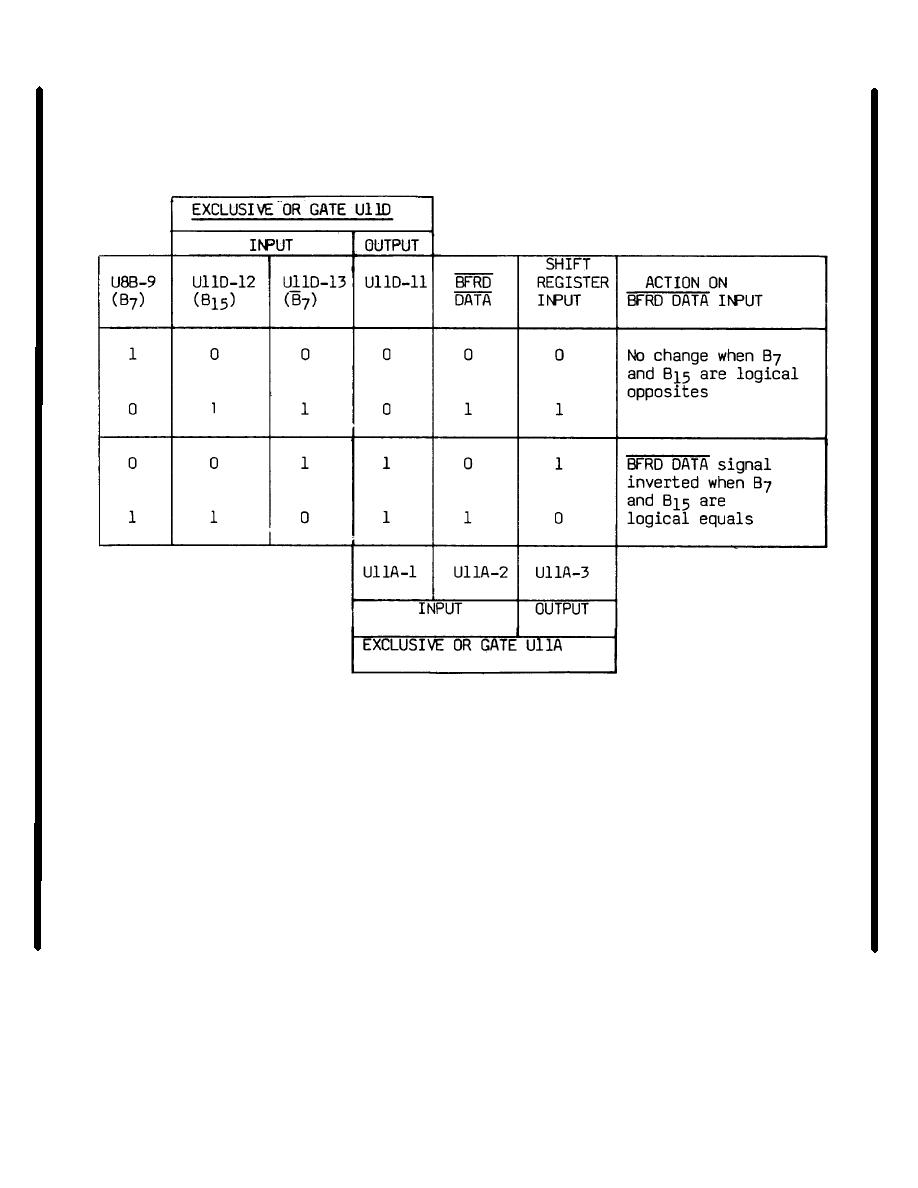
at U3-10; B7 is at U8B-9 and B15 at U4B-9. Bits B7
failure occurs. In addition, when the randomizer is
(U8B-8) and B15 (44B-9) are fed back through exclusive
inhibited a monitor circuit is activated causing CR2, a
OR gates U11D and U11A to control the data input at
yellow digital randomizer LED, to illuminate.
U8A-2. For every clock cycle, each data bit is shifted
(1) The scrambler circuits consists of a
forward one stage (B1 becomes B2, etc); B14 becomes
15-stage shift register (U8A, U3, U8B and U4B) with
B15, the new output bit. At the same time a new B1 is
shifted in a U8A-2; it is the next BFRD DATA bit fed
feedback from U4B-9 and U8B-8 through exclusive OR
gates U11D and U11A. The BFRD DATA input signal
through U11A. The action of U11A on the BFRD DATA
bit at U11A-2 is determined by the logic state of signals
(P1-T) is applied through U11A to the first stage (U8A)
of the shift register.
The clock signal (BFRD
Change 6 2-16.7
|
|
Privacy Statement - Press Release - Copyright Information. - Contact Us |