 |
|||
|
|
|||
|
Page Title:
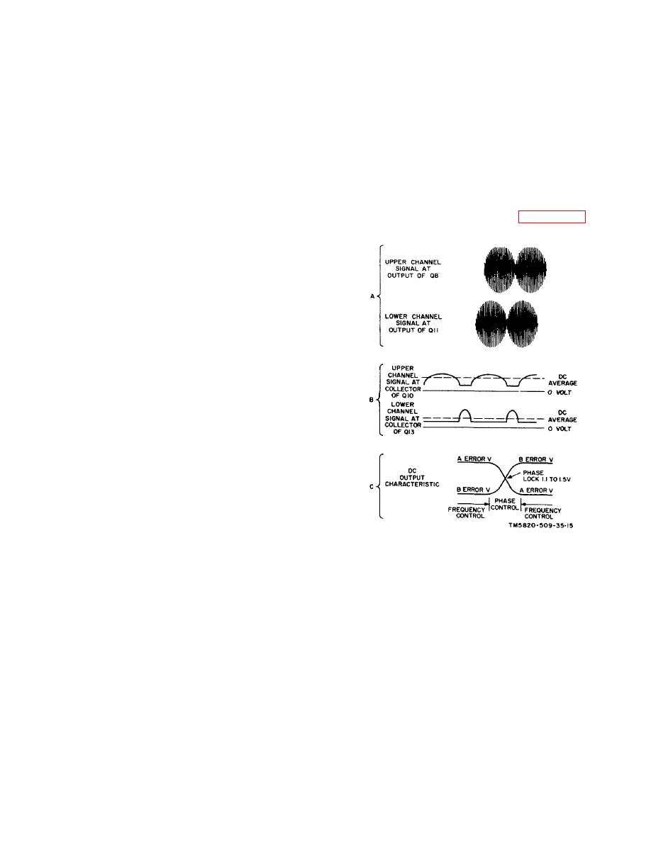
Figure 2 -15 Discriminator Circuit Waveforms. |
|
||
| ||||||||||
|
|  TM 11-5820-509-35
consists of the circuits associated with transistors Q8,
essentially drift-free output frequency at Q22 This output
Q9, and Q10, while channel B consists of the circuits
is routed through the bandpass filter consisting of
associated with transistors Q11, Q12, and Q13.
capacitors C105 through C109 and inductors L24
Selection of these transistors into matched pairs and the
through L26 to remove any spurious frequencies that
careful adjustment of bias and coupling components in
may have been in-troduced in the desired signal due to
these two channels assures nearly identical stage gains
mixing. The 700- to 601-kHz signal is clipped by limiter
in each of the two signal paths. Capicitor C21 and
CR7-CR8 to form a squarewave that is coupled to the
resistor R34 form a phase-shift network in the reference
discriminator circuit.
signal path from follower Q23 to the input of Q11. The
d. The O.9- to 1.8-MHz signal from limiter Q19 is
reference signals are summed with the unshifted output
routed through follower Q24 before being heterodyned
of clipper CR9-CR15 in both channels and the resulting
in diode quad mixer CR10 with the 5-to 14-MHz signal
signal at the output of Q8 and Q11 is similar to the
from Q18 in signal data translator A3. Since each of
waveform shown at the top of figure 2-15.
The
these input signals is variable (depending on the setting
repetition rate of these two envelopes is
of the KILOCYCLES indicator on the front panel of the
receiver-transmitter), the output of mixer Q10 is also
variable and may be any 100-kHz channel between 3.2-
and 13.1-MHz. This output frequency is routed through
follower Q25 and further mixed in diode quade CR11
with the hf oscillator signal from Q5 of signal data
translator A3. The difference-frequency at the output of
mixer CR11 is also variable and may be any 1-kHz
channel between 601- and 700-kHz.
This signal
contains an increment of hf oscillator error frequency.
The mixer output is amplified by Q26, filtered by the
circuit consisting of capacitors C169 through C177 in
association with inductors L29 through L32. Further
amplification is obtained by Q27 before routing the
signal to forward-limiting clipper CR9-CR15.
The
squarewave output of this clipper is applied to both
channels of the discriminator circuit.
e. The discriminator circuit has two modes of
operation: the frequency control mode, and the phase
control mode. When the hf oscillator output frequency
is within 50 kHz of the reference standard the
discriminator is said to be in the frequency control mode
and it compares the 601-to 700-kHz reference signal
from follower Q23 with the 601- to 700-kHz(plus hf
oscillator error) signal from clipper CR9-CR15. The
Figure 2 -15 Discriminator Circuit Waveforms.
resulting dc output is applied to the varicap control
circuit of signal data translator A3 to reduce the hf
equal to the difference between the two input
oscillator error toward zero.
When the difference
frequencies and represents the frequency error
between the hf oscillator output frequency and the
associated with the hf oscillator. Either envelope may
reference signal is less than approximately 5 kHz, the
lead the other along the time base, depending upon
discriminator assumes the phase control mode. In this
whether the hf oscillator frequency is higher or lower
mode, the circuit monitors the changing phase-
than the reference frequency. The outputs of amplifiers
difference between the two input signals and corrects
Q8 and Q 11 are further amplified by Q9 and Q12
the error voltages until this phase-difference approaches
respectively and the individual signals are then detected
zero. When the phase error is zero, the hf oscillator
by diodes CR3 and CR4. In the frequency control
output frequency is identical with the reference oscillator
mode, the leading edge of the envelope in each channel
output frequency. Discriminator channel A
is used to trigger transistor-pair Q10-Q13 so that they
alternately conduct. These transistors operate as a
bistable multivibrator with a switching rate equal to the
repetition rate of the envelope in each channel. The
resulting clipped
2-30
|
|
Privacy Statement - Press Release - Copyright Information. - Contact Us |