 |
|||
|
|
|||
|
Page Title:
Signal Data Translator CV-1377A/PRC-47 (A8A3) |
|
||
| ||||||||||
|
|  TM 11-5820-509-35
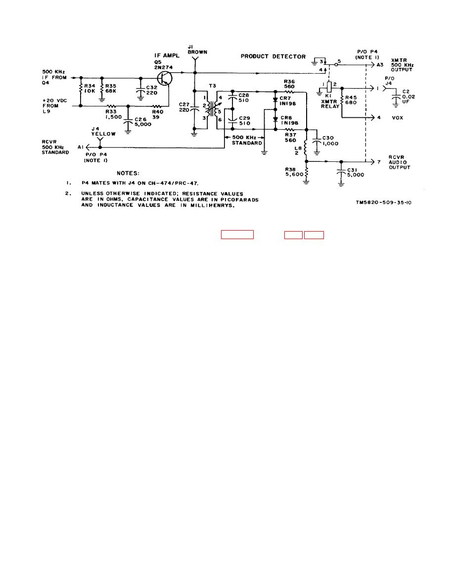
Figure 2-10. If. Amplifier and Product Detector Circuit, Schematic Diagram.
2-11. Signal Data Translator CV-1377A/PRC-47 (A8A3) (fig. 2-11 through 2-14, 7-11)
hf oscillator signal is again divided with part of it being
a. Signal data translator A3 contains isolation and
routed to follower Q12 and the remainder being applied
amplifier circuits, transmit sod receive mixer circuits, the
to follower Q13. The appropriate output of these circuits
tuned rf amplifier and driver stages, and the hf oscillator
is controlled by the bias voltage that is applied to either
and buffer amplifier. Follower Q2 isolates the output of
the +20 vdc rcvr input or to the +20 vdc xmtr input as B
buffer amplifier Q21 and routes the hf oscillator signal
+ relay K5 on the main chassis is operated. Application
through amplifiers Q3 and Q4 to follower Q5 and to the
of this bias voltage to Q12 as the receive mode is
oscillator control circuits (pare 2-14d ). This 2.5-to
selected enables the follower and places a forward bias
12.499-MHz signal branches at the emitter of follower
on CR6 that disables this gate. The hf oscillator signal
Q2 and is amplified by Q6 and Q7 before being routed
is then routed to the receiver mixer (Q11). When the
to the transmitter and receiver mixer circuits by follower
transmit mode is enabled, +20 vdc smtr input from
Q8. At the emitter of Q8, the
connector P1-2 is applied to follower Q13 and a forward
bias is placed on diode CR5. The transmit mixer input
is made operative and the receiver mixer is disabled.
2-21
|
|
Privacy Statement - Press Release - Copyright Information. - Contact Us |