 |
|||
|
|
|||
|
Page Title:
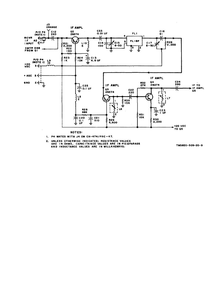
Figure 2-9 If. Amplifier Circuit, Schematic Diagram. |
|
||
| ||||||||||
|
|  TM 11-5820-509-35
Figure 2-9 If. Amplifier Circuit, Schematic Diagram.
connected diode mixers that are alternately switched on
and off at the 500-kHz standard signal rate. The receive
amplifier Q4 is further amplified by Q5. The output of
500-kHz standard signal is present only when the
this common-emitter amplifier is routed to the normally-
receive mode is enabled and there is no 26.5-volt vex
open contacts of transmit relay K1, and then by way of
signal applied to 500-kHz relay K4.
The audio
transformer T3 to the product detector. In the transmit
component at the output of the product detector is the
mode, the 26.5-volt dc potential from vox relay AlK1
difference between the instantaneous values of the
operates transmit relay Kl and routes the transmit 500-
incoming lower-sideband if. signal and the receive 500-
kHz if. output from P4-A3 to the transmit mixer of signal
kHz standard signal. This audio output is routed through
data translator A3. When the receive mode is selected,
the low-pass filter consisting of C30, C31, and L8 to
however, the receive if. signal from amplifier Q5 is
remove the remaining if. component before further
routed to the product detector circuit by transformer T3.
amplification by circuits in audio frequency amplifier A1
Product detector CR7-CR8 consists of two push-pull
2-20
|
|
Privacy Statement - Press Release - Copyright Information. - Contact Us |
