 |
|||
|
|
|||
|
Page Title:
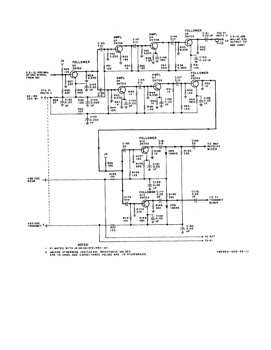
Figure 2-11. Isolation Amplifier Circuits, Schematic Diagram. |
|
||
| ||||||||||
|
|  TM 11-5820-509-35
Figure 2-11. Isolation Amplifier Circuits, Schematic Diagram.
L100. Since the enabling bias @ +20 vdc xmtr) is not
applied, gate CR2 also remains enabled and this signal
applied to the emitter of receiver mixer Q11 when the
is routed through follower Q9 to the if. amplifier circuits
receive mode is selected. The incoming receive rf
of amplifier-modulator A2. During receiver operation
signal from second rf amplifier V2 is routed through the
follower Q14 and amplifier Q15 are unbiased and
normally-closed contacts of relay K1, through follower
remain disabled. As the transmit mode is selected,
Q10, to the base of receiver mixer Q11. The collector
however, the +20 vdc xmtr bias is applied to P1-2 and
of this transistor is tuned to the difference-frequency of
transistors Q14 and Q15 are enabled. Forward bias is
these two signals by the parallel-tuned circuit consisting
also applied to gate CR2 so that it is disabled and
of capacitors C167 through C169 and inductor
2-22
|
|
Privacy Statement - Press Release - Copyright Information. - Contact Us |
