 |
|||
|
|
|||
|
Page Title:
Transmitter Second Rf Amplifier Module A7 |
|
||
| ||||||||||
|
|  decreasing the total capacitance. The rf
collector is coupled through BAND switch
input to module A8 can be measured at
S1A to either the low- or high-band tuned
test jack J2.
output circuit.
d. Inductor L2 and capacitors C6 and
b. Separate tuned output circuits are
C7 (in the main frame (fig. 88)) form a
used for the high and low bands. Switch S1
filter in the +10-volt regulated input to
selects the circuit when the BAND switch
module A8.
is positioned.
(1) Low band The low-band tuned out-
put circuit consists of inductor T3,
Module A7
trimmer capacitor C9, and ganged
tuning capacitor C1B (fig. 88),
which is varied by the tuning con-
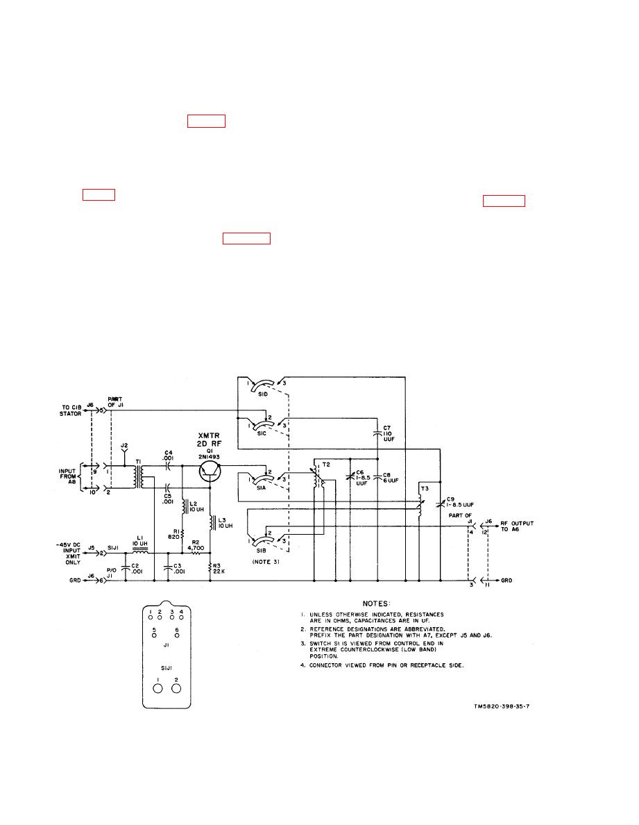
Transmitter second rf amplifier module
A7 amplifies the signal from transmitter
trols on the front panel. The output
is applied from a tap on T3 through
first rf amplifier module A8 (para 16).
S1B to A6.
Module A7 consists of a single transistor
amplifier, a BAND switch, and a tuned
(2) High band. The high-band tuned
output circuit.
output circuit consists of the pri-
a. The output signal from A8 is coupled
mary of transformer T2, fixed
from the top of the center-tapped second-
capacitor C8, trimmer capacitor
ary of T1 through coupling capacitor C4
C6, and ganged tuning capacitor
to the emitter of Q1 and from the bottom
CIB. The output is applied from
of the secondary through coupling capac-
the secondary of T2 through SIB
itor C5 to the base of Q1. The output at the
to A6.
|
|
Privacy Statement - Press Release - Copyright Information. - Contact Us |