 |
|||
|
|
|||
|
Page Title:
First, Second, and Third Rf Amplifiers V102, V103, and V104 on Transmit |
|
||
| ||||||||||
|
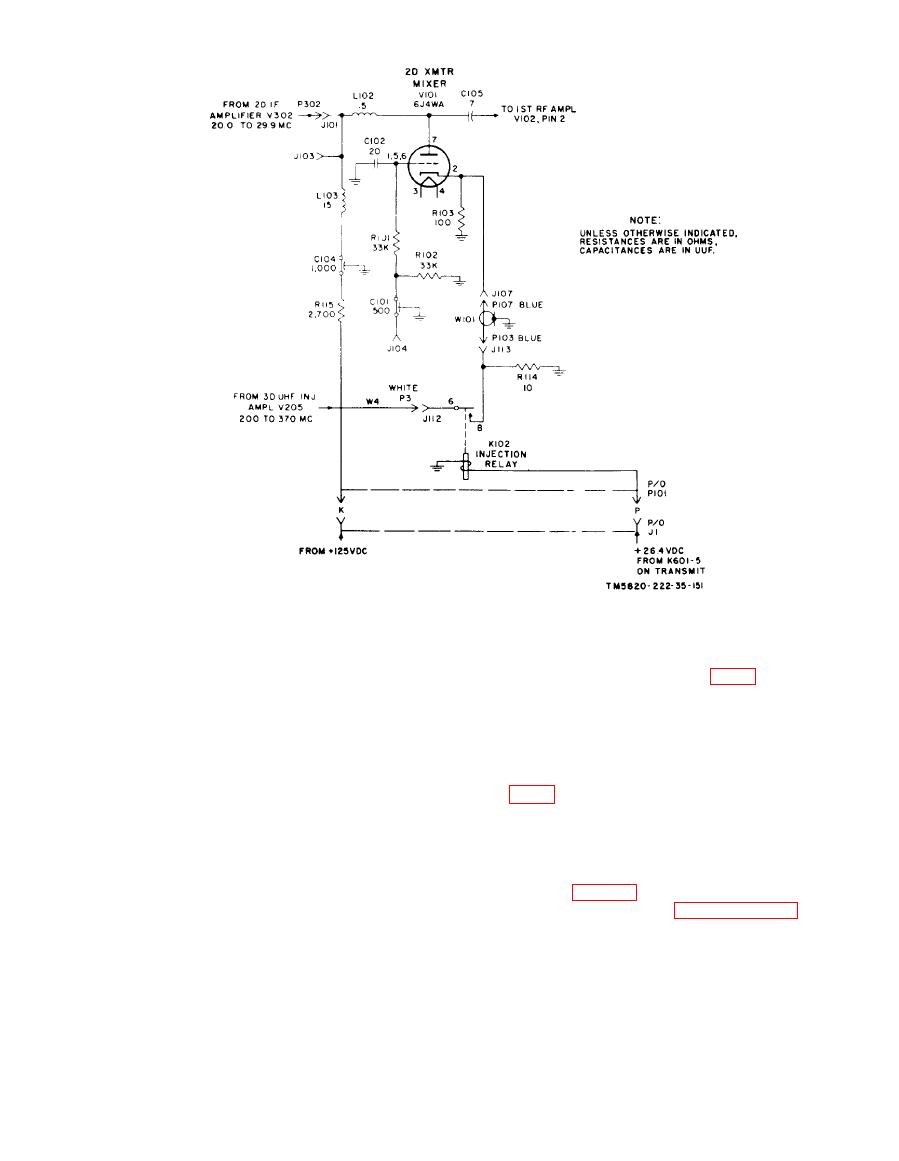
|  and L102. J103 is a test point for measur-
prevents the dc plate voltage on V101 from
ing the plate voltage or the 20.0- to 29.9-
being grounded through Z101 (fig. 5) and
mc signal applied to the plate of V101. Rf
couples the 225.0- to 399.9-mc from the
choke L103 and bypass capacitor Cl04 de-
plate of V101 to first rf amplifier V102.
couple rf from the +125-volt dc supply.
Capacitor C102 grounds rf at the grid of
V101. Resistors R101 and R102 are the
V102, V103, and V104 on Transmit
grid-leak circuit to ground. Jack J104 is
a test point for measuring grid bias on
V101. Bypass capacitor C101 provides a
Coupling capacitors C105 and C110 cou-
l o w - i m p e d a n c e path to ground for rf
ple the rf signal to the cathode of V102. The
signals. Resistors R103 and R114 provide
rf signal receives three stages of rf ampli-
t h e correct termination for injection
fication and is applied to transmitter
cables W101 and W4. On transmit, the +26
driver V105 (para 55). The rf amplifiers
vdc from K601 energizes R102.
function as described in paragraphs 13
c. The 200- to 370-mc uhf injection fre-
through 15 with the following exceptions:
quency and the 20.0- to 29.0-mc first if.
are heterodyned in V101 to produce an out-
tacts 2-3 open) to remove the directional
put rf within the 225.0- to 399.9-mc range.
coupler from the input circuit of first rf
(The band of frequencies between 220-225
amplifier V102.
mc is not used.) Blocking capacitor C105
|
|
Privacy Statement - Press Release - Copyright Information. - Contact Us |