 |
|||
|
|
|||
|
Page Title:
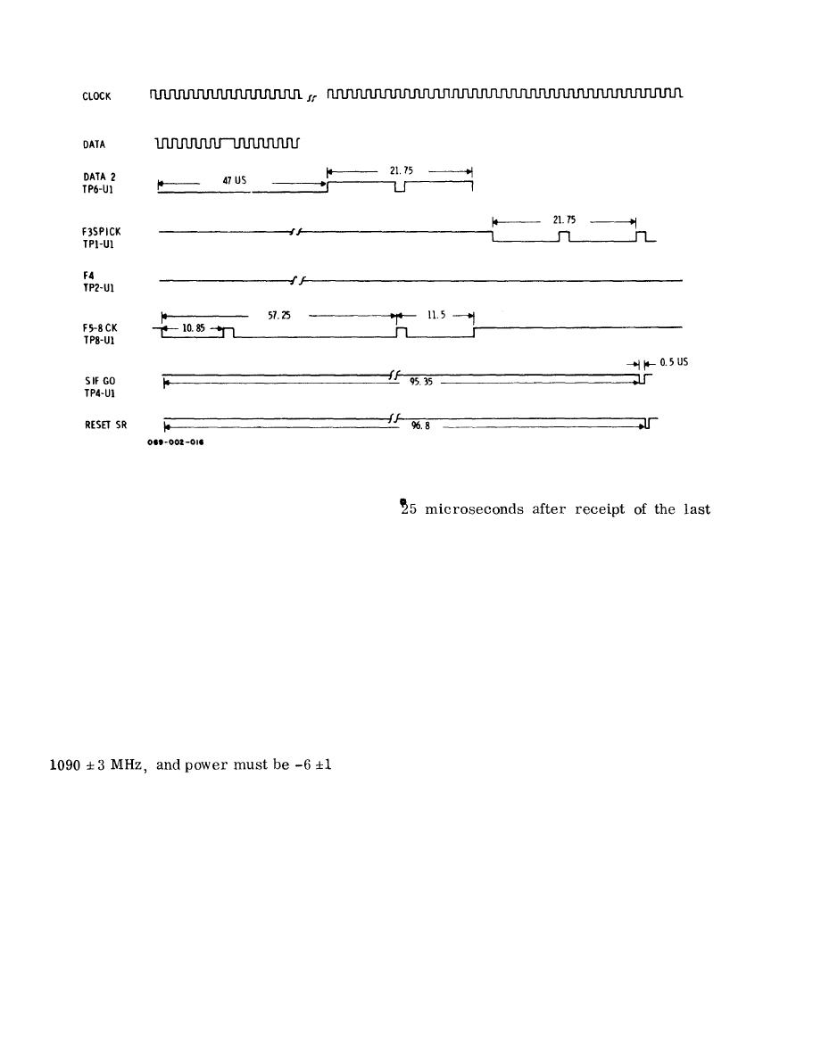
Figure 2-5. Timing Diagram, Decode Cycle (SIF Reply Code 7777) |
|
||
| ||||||||||
|
|  TM 11-4920-296-14&P
T i m i n g Diagram, Decode Cycle (SIF Reply Code 7777)
microseconds) VIDEO GATE signal (U3-
T P 3 ) . A f t e r the delay period, the VIDEO
reply pulse.
G A T E from U3-TP3 is applied to the rf
2-32. The DATA (at U3-TP1) is clocked
module and gates the local oscillator for 8.5
m i c r o s e c o n d s , activating the receive r cir-
t h r o u g h shift-register stages of U2, and
cuits. In addition to these previous actions,
appears at U1-TP6 as the DATA-2 input to
the P3 pulse triggers generation of a REPLY
shift-registers of U1. When the DATA-2 bit
GATE (U3-TP4), which inhibits any interro-
corresponding to the F1 reply pulse appears
gations during the decode cycle.
at a specified tap on the last shift-register
s t a g e , a parity strobe is generated. This
2-31. N o w during the decode cycle, when
strobe enables a parity circuit to then check
reply pulses (at 1090 MHz) are received from
for absence or presence of the reply frame
t h e transponder under test, they are down-
a n d coding pulses (as applicable), The
converted to 30 MHz, detected (demodulated)
p a r i t y circuit compares the reply pulses re-
in the rf module circuits, and their frequency
ceived against a reply code set by by posi-
and power are checked. (Frequency must be
tioning of the CODE SELECT switches on
the test set front panel; the received reply
d B m . ) Provided the reply pulses meet the
must match that set by the CODE switches,
f r e q u e n c y / p o w e r requirements, they are
to produce an ACCEPT condition. Addition-
s e n t to the digital section as the REPLY
ally, F3, F4, and F5-to-F8 parity compari-
SAMPLE (U3-TP10). At this time, the reply
sons are made for pulses following the F2
pulse width is normalized to form the DATA
p u l s e . If all comparison conditions are met
s i g n a l s at U3-TP1, and the CLOCK is
(at the parity strobe time), a SIF GO strobe
d e s y n c h r o n i z e d with the DATA to insure
i s generated (U1-TP4) and sent to the
c o r r e c t loading of the DATA into shift-
evaluator board U4 circuits.
register stages. Receipt of reply pulses also
2-33. As the F1 pulse of the DATA-2 signal
causes "hold-open" of the VIDEO GATE (at
is shifted past the parity-strobe tap of U1,
U3-TP3) such that the local oscillator (and
a RESET SR pulse (U1-TP10) is generated
receive function) will be enabled for at least
|
|
Privacy Statement - Press Release - Copyright Information. - Contact Us |
