 |
|||
|
|
|||
|
Page Title:
Figure 2-4. Timing Diagram, Encode Cycle (SIF Mode 3) |
|
||
| ||||||||||
|
| 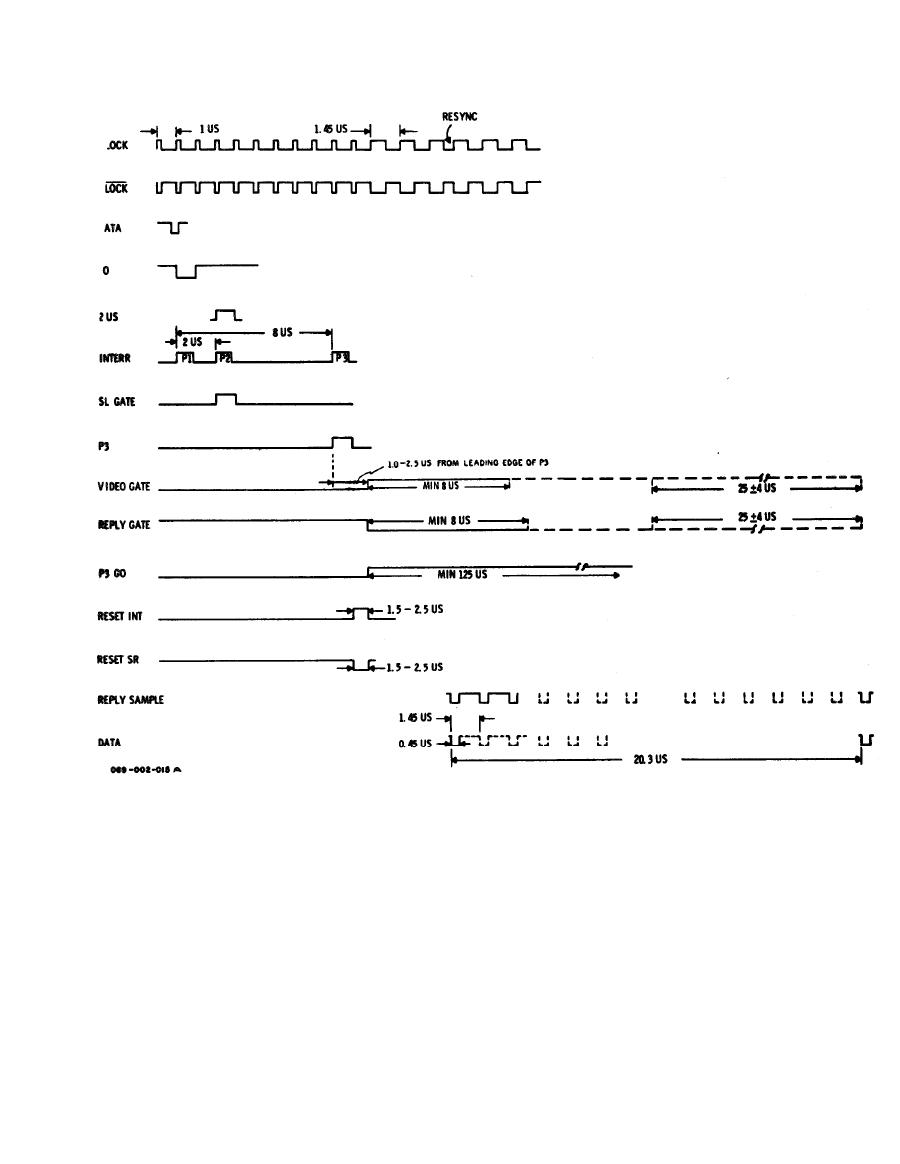 TM 11-4920-296-14&P
circuits of the rf module, to develop the side
to initiate the P3 interrogation pulse; the
lobe function.
specific register tap-out point for the P3
pulse (determined by the MODE selection
2-30. The P3 pulse so developed in the dig-
switch) produces the specified spacing of
ital circuits performs several functions
the P1 and P3 pulses for the mode selected.
within those modules. It causes the RESET
INT signal (U1-TP5) and the RESET SR sig-
2-29. The three pulses (P1, P2, and P3)
nal (U1-TP10) to clear the register stages of
are regenerated into standard-width INTERR-
all encode-cycle data. The trailing edge of
ogation pulses (at U2-TP8) and are fed to
the P3 pulse (at U3-TP6) causes changing of
the rf module circuits where they gate
the CLOCK rate to 690 kHz for the fol-
(modulate) the 1030-MHZ rf transmitter
c i r c u i t s . Additionally, the P2 pulse is
lowing decode period. A l s o , the P3
applied from U4-TP1 to the SLS GATE
pulse triggers a delayed (1.5 - 2.5
|
|
Privacy Statement - Press Release - Copyright Information. - Contact Us |
