 |
|||
|
|
|||
|
Page Title:
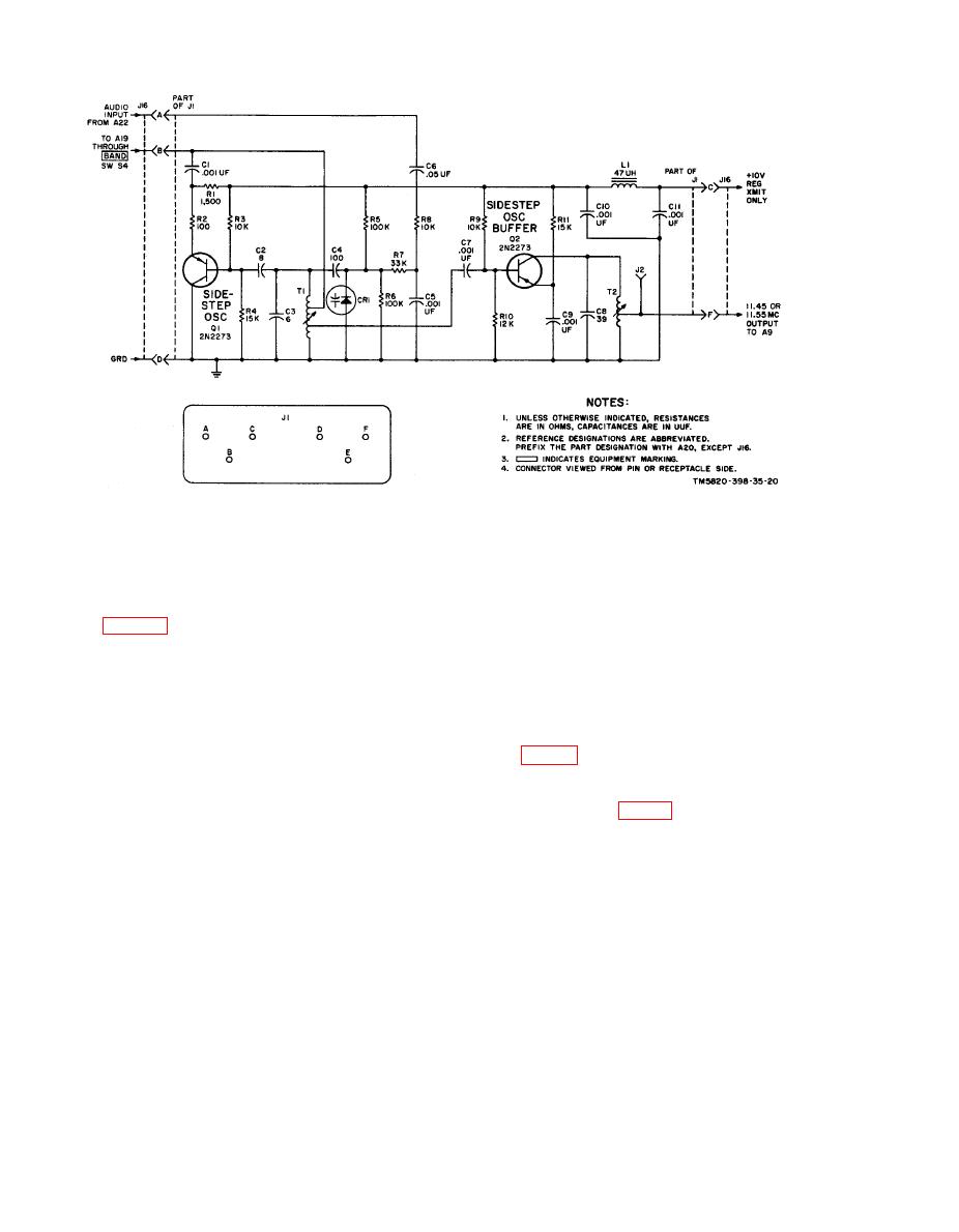
Figure 8. Sidestep oscillator module A20, schematic diagram. |
|
||
| ||||||||||
|
|  isolation, and proper match for the vfo
quency of the vfo. The automatic
signal applied to the fss. An output from
phase control voltage from module
the vfo is directly fed to receiver mixer
All can be measured at test jack
A5 (para 8) and heterodyned with the in-
J3.
coming signals to produce the 11.5-mc if.
(3) Resistors R1 and R2 develop the
base bias for Q1. Resistor R3 is the
The third vfo output is applied to trans-
mitter mixer Q2.
emitter swamping resistor. The rf
signal at the tuned circuit can be
a. VFO Q1.
measured at test jack J4.
(1) Collector-to-emitter fee db a c k
(4) Capacitor C8 (in the main frame
through capacitor C2 and inductor
T1 maintains oscillation in Q1. The
on the automatic phase control
tuned circuit consists of inductor
voltage line. Capacitor C9 (in the
Tl, trimmer capacitor C9 fixed
main frame (fig. 88) is an rf bypass
capacitor C10, capacity diode CR1,
and ganged tuning capacitors C1D
capacitor on the +10-volt regulated
input line.
C1E which are varied by the tuning
controls on the front panel. Trim-
b. Frs Buffer Amplifier Q3.
mer capacitor C8 controls the ef-
(1) The output from the vfo is applied
fect of CR1.
through isolation resistor R11 and
(2) Input error signals from the fre-
coupling capacitor C11 to the base
quency synthesizer system are
of Q3. Transformer T2 couples the
applied through a filter network
output of this stage to the input of
consisting of inductor L4 and ca-
the fss.
pacitor C7, and through isolating
(2) Voltage-divider resistors R12 and
resistor R9 to capacitance diode
R13 develop the fixed base bias for
CR1. The capacitance of CR1 var-
Q3. Resistor R14 is the emitter
ies directly with the applied error
swamping resistor. Capacitor C12
voltage to correct the output fre-
is the rf bypass capacitor for the
18
|
|
Privacy Statement - Press Release - Copyright Information. - Contact Us |
