 |
|||
|
|
|||
|
Page Title:
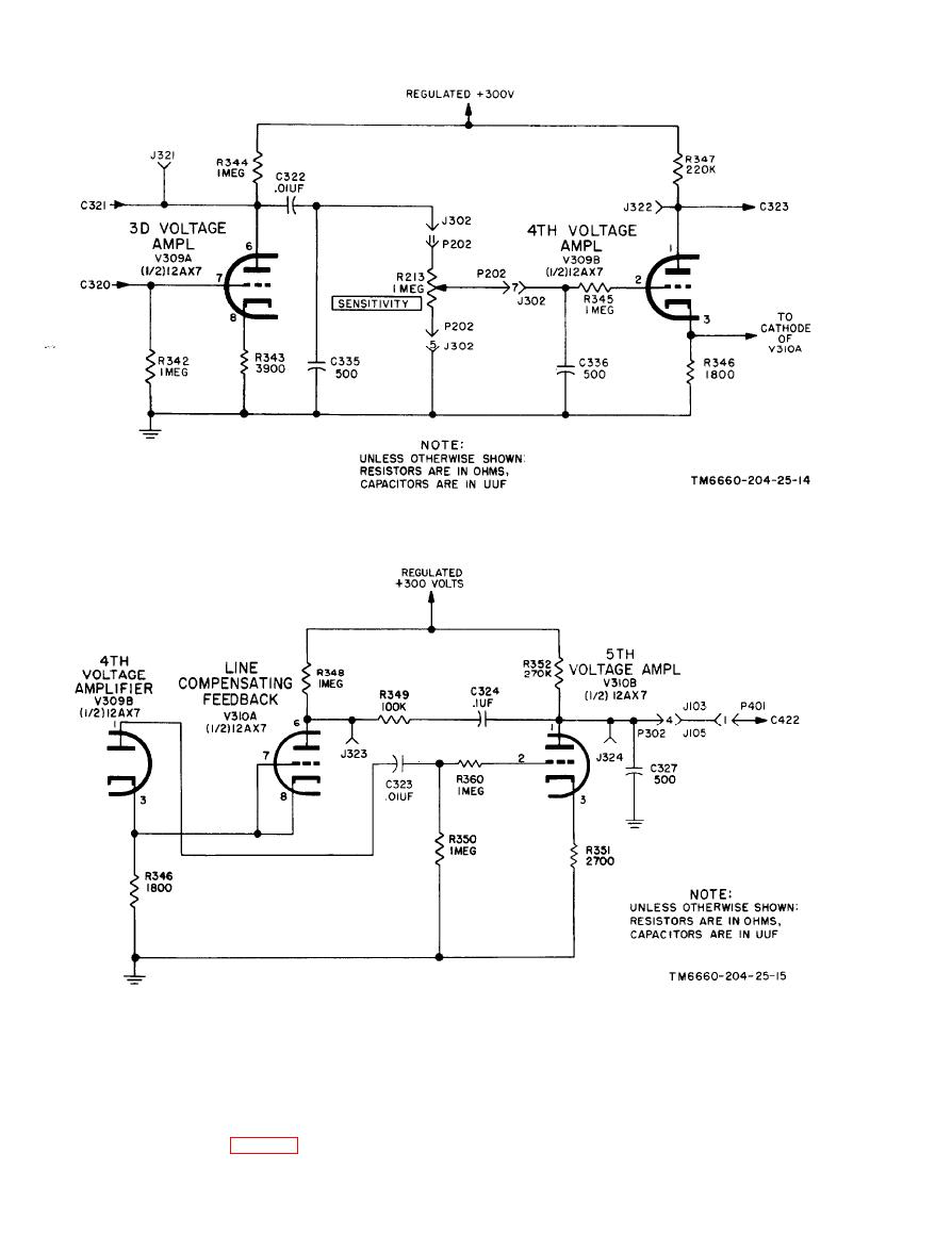
Figure 213. Third and fourth voltage amplifiers, simplified schematic diagram, |
|
||
| ||||||||||
|
|  TM 11-6660-204-25
simplified schematic diagram.
b. The signal from the plate of first amplifier
amplified and appears across plate-load resistor
tube V308A is fed through coupling capacitor
R341. Self-bias is provided by cathode resistor
C319 to grid resistor R339 and the grid of second
R340, which is unbypassed to obtain negative
amplifier tube V308B (fig. 212). The signal is
feedback. The plate voltage of tubes V308A and
|
|
Privacy Statement - Press Release - Copyright Information. - Contact Us |
