 |
|||
|
|
|||
|
Page Title:
Figure 21. First and second rf amplifiers (20-70 mc), schematic diagram. |
|
||
| ||||||||||
|
| 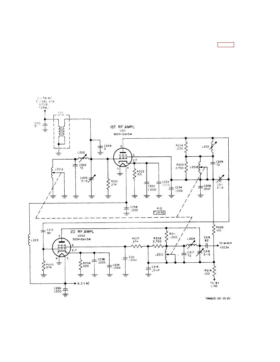 R202, which is bypassed by C232 and C233.
h e a t e r line. The voltage across the plate
Capacitor C234 is the screen grid bypass.
tuned circuit is coupled to the grid of sec-
The rf output voltage in the plate circuit
ond rf amplifier V202 through capacitor -
of V201 is developed across the parallel-
C212.
tuned circuit which consists of tuning in-
ductor L201B, capacitor C209, coil L203,
The signal voltage from first rf amplifier
and trimmer capacitor C211. Resistors
V 2 0 1 is amplified by second rf amplifier
R203 and R204 are used to load the plate
V202 and coupled to mixer stage V203A.
t u n e d circuits. Resistor R209 and capac-
The input signal voltage is developed
itor C208 provide decoupling for the plate
a c r o s s grid resistor R205. Cathode bias
c i r c u i t . Bypass capacitor C258 and choke
i s developed by the voltage drop across
L223 are connected in the 6.3-volt bus and
R 2 0 6 , which is bypassed by C238 and
prevent rf currents from circulating in the
C239.
F i g u r e 21. First and second rf amplifiers (20-70 mc), schematic diagram.
50
|
|
Privacy Statement - Press Release - Copyright Information. - Contact Us |
