|
| |
TM 11-5820-890-30-5
6-7.
SELF-TEST. Continued
Several displays are generated to indicate the results of the test. They are:
All display segments are lit to check display operation.
“Gd” display indicates self-test was passed.
“F1” display indicates a microcontroller failure.
“F2” display indicates an analog channel failure.
Self-test is always executed on turn-on. It will repeat the self-test as long as the FCTN switch is set to TEST.
The front panel displays are lit first. A series of “ones” are sent on the DISPLAY DATA line to light all the display
segments. This pattern is sent twice. The display segments are lit for about 3 seconds.
Next, the microcontroller ROM is checked. It is checked by summing all of the bytes in ROM except the last two
and comparing the sum to the last two bytes in ROM. If they are the same, the ROM code, address bus, data bus,
and access lines are verified. Self-test continues with the next check. If not, “F1” is displayed.
If the ROM check passes, the RAM is checked. All RAM addresses are checked by writing and reading a value at
each address. When checked at turn-on, all RAM values are set to zero. When the FCTN switch is set to TEST,
the values in RAM are retained and restored. If the RAM check passes, the RAM, address bus, data bus, and
access lines are verified. If any RAM address fails, "F1" is displayed.
The analog channel operation is checked next. All three radio transmit/receive paths are checked. Radio channel
3 is checked first, followed by radio channel 2, and then radio channel 1. The channels are tested by sending a
carrier signal on the FSK DATA line and changing its frequency from 3200 Hz to 2560 Hz. The 2880 DET-N line
should stay at logic 0. The RCV DATA line should change logic states with each frequency change.
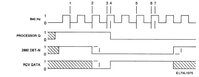
A channel test is started by setting the PROCESSOR Q line to logic 1. See figure 6-6. The test is delayed until
there is no activity on the selected channel and a negative 640-Hz clock edge is detected (1). This ensures that
the PROCESSOR Q line is set to logic 1 (3200 Hz). The carrier is turned on (2). After two clock periods (3), about
3 ms, the first check is made (4). The 2880 DET-N line should be at logic 0. The RCV DATA line should be at
logic 0. If both pass, the PROCESSOR Q line is set to logic 0 (2560 Hz). After a second delay (5), and two clock
periods (6), the checks are repeated (7). The 2880 DET-N line should beat logic 0. The RCV DATA line should be
at logic 1. If both pass, the carrier is turned off and the next channel is checked. If any failures are detected, "F2"
is displayed.
If all self-test checks are passed, “Gd” is displayed.
Figure 6-6. Analog Check Timing.
6-9
|

