|
| |
TM 11-5820-890-30-5
6-6.
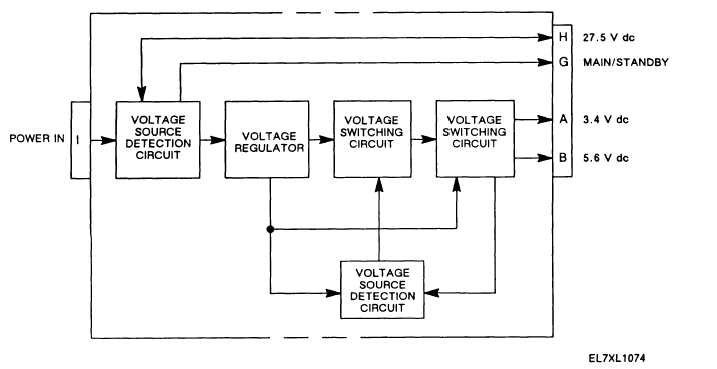
POWER SUPPLY (7A5).
The power supply operates using the switched 27.5 V dc from the mounting adapter. It will operate with an input
voltage between 18.5 and 32 V dc. It requires no more than 1 A. Its outputs are 5.43 to 5.77 V dc (5.6 V dc
nominal) and 2.9 to 3.9 V dc (3.4 V dc nominal). Both outputs are overcurrent protected.
The power supply can receive its input power from either pin I or pin H. See figure 6-5. When the control-monitor
is connected to the radio, 27.5 V dc is present at connector J1 pin F. See figure FO-17. It is routed to pin I of the
power supply. The voltage source detection circuit pulls the MAIN/STANDBY line to logic 1. The 27.5 V dc is
output through pin H to connector J3 pin F. When the control-monitor is the second one in the system, it receives
power at connector J3 pin F. It is input to the power supply at pin H. This causes the voltage source detection
circuit to pull the MAIN/STANDBY line to logic 0.
The power supply operates as a switching voltage regulator. The output of the switching circuit is compared to a
reference voltage. The output voltage regulator circuit uses the difference in the two voltages to set the switching
rate. This rate is adjusted until there is no difference between the reference voltage and the sampled output
voltage.
Overcurrent protection is also provided. If 100 mA on the 5.6 V line or 400 mA on the 3.4 V line is exceeded, the
power supply reduces both outputs to 0 V.
Figure 6-5. Power Supply Functional Block Diagram.
6-7.
SELF-TEST.
The self-test function checks the following:
Front panel displays.
Microcontroller RAM and ROM.
Analog channel operation.
6-8
|