 |
|||
|
|
|||
|
Page Title:
The 0.1 MHz and 1 MHz divide-by-ten counter |
|
||
| ||||||||||
|
|  TM 11-5820-695-35
registers count down the clock pulses until the reset
enable signal from variable 2 frequency divider 1A14A6
is received and the registers contain the unique number
(1 MHz register contains 0100-decimal 4, 0.1 MHz
register contains 0100-decimal 6). After the unique
number count, the initialize, inhibit, and preload
sequence (8 counts) takes place. During the initialize,
inhibit, and preload periods, the clock pulses are
prevented from being counted. The 0.1 MHz and 1 MHz
register stages are set to all ones during the initialize
c. The following is a description of the divide by-
period, the count (all ones) in the counter registers is
ten registers (BCD down counters).
As stated
modified in accordance with the 1 MHz and 0.1 MHz
previously, the output from stage Z12 of the 0.1 MHz
thumbwheel switch settings. After the preload period,
divide-by-ten counter register triggers the first stage of
the clock pulse are no longer inhibited and the count
Z18 of the 1.0 MHz divide-by-ten counter registers.
(determined by thumbwheel switch settings) in the
Assume that integrated circuits Z18, Z15, Z17, and Z18
registers is decremented by the incoming clock pulses.
are all reset (0000). The first negative going transition
The counter registers count down through zero until the
from Z12 sets Z1 and Z18 (1001: ). To set a flop-flop
reset enable signal is received from 1A14A6 and the
type 950 pin 4 must be at a 0 volt level; to reset the flip-
unique number again appears in the registers. The
flop, pin 10 must be at a 0 volt level. If the count is
cycle then repeats as described above.
0000, only Z13, Z17, Z18 are conditioned to be set;
however, since Z15 does not change, no transition will
b. The 0.1 MHz and 1 MHz divide-by-ten counter
be applied to Z17. The second negative-going transition
registers on board A2 are binary coded decimal (BDC)
from Z12 resets Z18 (1000). At this time, the input to
counters. The 0.1 MHz divide by-ten counter register is
pin 9 of NAND gate Z11B is a low (0 volt) level and pin
comprised of integrated circuits Z6 (least significant bit)
8 is a high (5 volt) level; this now satisfies the two ones
Z8, Z710, and Z12 (most significant bit). The 1 MHz
requirement of NAND gate Z16D, since pins Z16D-12
divide by-ten counter register is comprised of integrated
and 13 are both high.
The third negative-going
circuits Z18 (least significant bit), Z16, Z17, and Z18
transition from Z12 sets D18, Z16, and Z.17 and resets
(most significant bit). The registers are cascaded: the
Z1 (0111). The fourth negative-going transition from
clock pulses are applied to the first stage D6 -of the 0.1
Z12 resets Z13 (0110).
The fifth negative-going
MHz register; the output stage 112 of the 0.1 MHz
transition from Z12 sets Z13 and resets 715 (0101). The
register triggers the first stage Z13 of the 1 MHz
sixth negative-going transition from Z12 sets Z13 and
register; the output stage Z18 of the 1 MHz register is
Z15 and resets Z17 (0100). The eighth negative-going
inverted through count inverter Z14C and the output
transition from Z12 resets Z13 (0010). The ninth
.(count) is applied to the first stage of the 10 MHz
negative-going transition from Z12 sets Z13 and resets
register in variable 2 frequency divider 1A14A5. The
Z15 (0001). The tenth negative-going transition from
0.1 MHz and the 1 MHz divide-by ten counter registers
Z12 resets Z13 (0000).
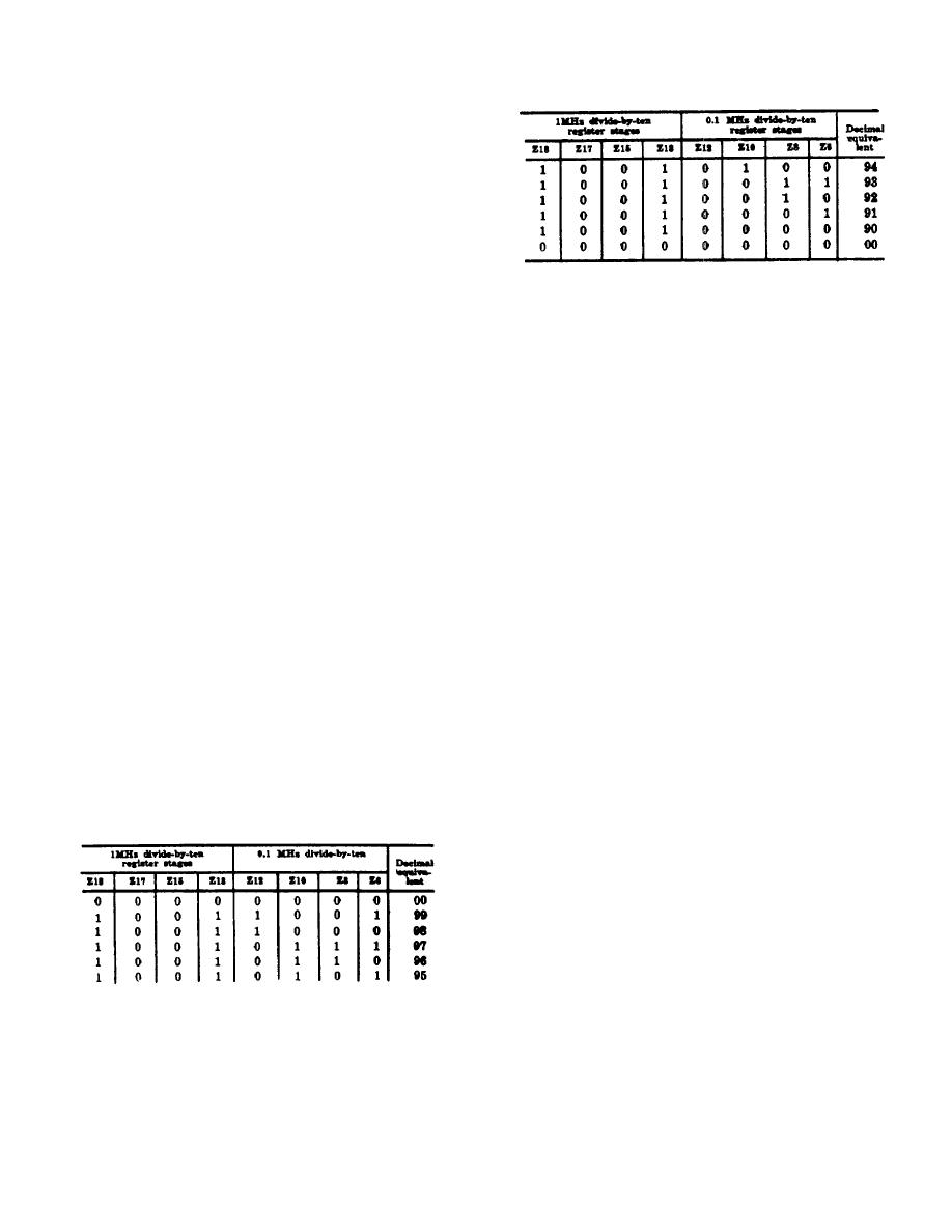
in 1A14A4 count down in accordance with the following
chart. It should be noted the chart lists the state of each
register stage for 99 through 90. For 89 through 00 the
d. Variable 1 frequency divider 1A14A4 divides the
standard binary logic regression applies.
if output frequency from 1A14A2 by 200 (one divide-by-
two flip-flop, and two divide by-ten counter registers).
Thing for the divide by-200 operation is shown in figure
2-18, part 1.
The clock pulses from Z1 are the if output frequency
from 1A14A2 divided by two. The waveform at pin 8
(set output) of each register stage is shown from the
time T. through T. (T is the period of the clock pulse).
Pin 11 of Z12 is also shown since the negative-going
transition of this output causes Z12 (input stage of the
second divide-by-ten counter) to trigger. The width of
the count signal at pin 8 of output inverter Z14C
2-98
|
|
Privacy Statement - Press Release - Copyright Information. - Contact Us |
