 |
|||
|
|
|||
|
Page Title:
Figure 6. Speech amplifier limiter module A22, schematic diagram. |
|
||
| ||||||||||
|
| 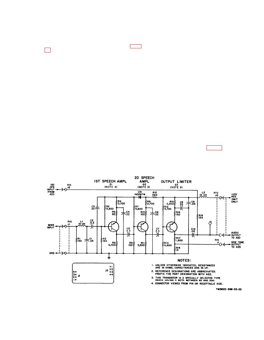 coupling capacitor C7 to the base of output
inversely with temperature; therefore, the
bias remains constant despite wide vari-
limiter Q3. The output limiter signal is
developed across collector load resistors
ations in temperature. Resistor R10 is the
R17 and R18. The audio output to A20 (para
emitter swamping resistor for Q2. The
combination of resistor R9 and capacitor
C10 while the sidetone output to receiver
C6 decouples the Q2 emitter circuit from
any extraneous noise signals. Resistor
audio module A25 is directly coupled from
the junction of resistors R17 and R18. A
R11 is the collector load for second speech
150-cps tone signal from the tone genera-
amplifier Q2.
c. Resistive divider R13 and R14 pro-
tor module is superimposed on the audio
output signal to the sso through isolation
vides base-to-emitter bias for output lim-
resistor R19.
iter Q3. Resistor R16 is the emitter
swamping resistor' for Q3. The combina-
b. Resistors R2 and R3 establish base-
tion of resistor R15 and capacitor C8 de-
to-emitter fixed bias for transistor Q1.
couples the e m i t t e r circuit from any
Resistor R5 is an emitter swamping re-
extraneous noise signals. The combination
sistor for Q1. The combination of resistor
of inductor L2 and capacitor C9 decouples
R4 and capacitor C4 decouples the emitter
the emitter from the +10-volt supply. Re-
circuit from the +10-volt supply. Resistor
sistor R12 is a power supply voltage drop-
R6 is the collector load for first speech
ping resistor. Capacitor C22 filters the
amplifier Q1. Resistor 11 is the collector
power supply voltage for transistors Q1
load resistor for second speech amplifier
and Q2. The audio output to module A20
Q2. The combination of resistors R7, and
can be measured at test jack J3. Capacitor
R8 and diode CR1 establishes base-to-
C10 (in the main frame (fig. 88)) is an rf
emitter bias for speech amplifier Q2. Be-
bypass capacitor on the +10-volt regulated
cause of the negative temperature coeffi-
input to modules A22 and A23.
c i e n t of diode CR1, the bias varies
15
|
|
Privacy Statement - Press Release - Copyright Information. - Contact Us |
