 |
|||
|
|
|||
|
Page Title:
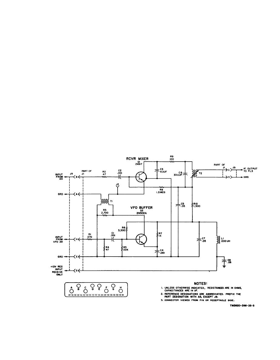
Figure 3. Receiver mixer module A5, schematic diagram. |
|
||
| ||||||||||
|
|  b. Receiver Fourth and Fifth If. Ampli-
the tuned circuit consisting of ca-
fiers Q4 and Q5. Transistors Q4 and Q5,
pacitor C9 and the primary winding
amplify the if. signal, and also limit strong
of transformer T1.
signals.
(2) The combination of resistors R2
(1) The out put of Q4 is developed
and R3, R7 and R8, and R11 and R12
across collector load resistor R17
develops base-to-emitter bias for
and is coupled through capacitor
Q1, Q2, and Q3 respectively. Re-
C12 to the base of fifth if. amplifier
sistors R4, R9, and R13 are emit-
Q5. The collector output of ampli-
ter swamping resistors. Capaci-
fier Q5 is developed across load
tors C3, C6, and C8 are emitter
resistor R21 and applied through
rf bypass capacitors for Ql, Q2,
coupling capacitor C 15 to the base
and Q3 respectively. Resistors R5
of receiver discriminator driver
and R10 are collector load resis-
Q6.
tors for amplifiers Q1 and Q2, re-
(2) Resistors R14 and R15, and R18,
spectively. Resistor R6 and capac-
and R19 develop base-to-emitter
itor C2 form a decoupling network
bias for Q4 and Q5 respectively.
between the +10-volt circuit of the
Resistors R16 and R20 are emitter
first if. amplifier and the other
swamping resistors and capacitors
stages. The input signal to module
C11 and C14 are the emitter bypass
A21 can be measured at test jack
capacitors for Q4 and Q5 respec-
J3.
Figure 3. Receiver mixer module A5, schematic diagram.
11
|
|
Privacy Statement - Press Release - Copyright Information. - Contact Us |
