 |
|||
|
|
|||
|
|
|||
| ||||||||||
|
|  TM
11-6660-204-25
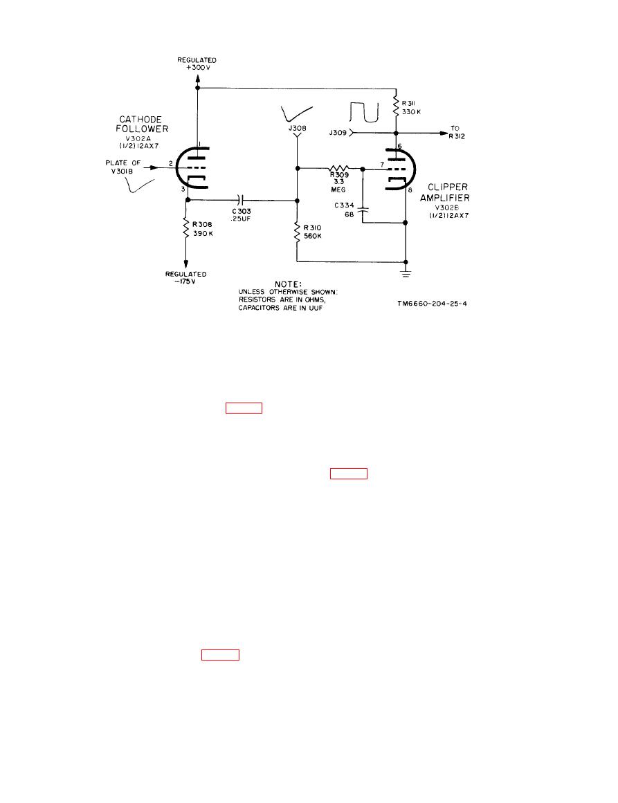
Cathode follower and clipper amplifier,
simplified schematic diagram.
b. Coupling capacitor C303 isolates the grid of
cause the high value of resistor R309 does not
tube V302B from the dc component of the cathode
allow the space charge on the grid to leak off
voltage of the preceding stage. The waveform
easily. The small value of capacitor C344 allows it
across resistor R310 is shown at J308 (fig. 23).
to be effective as a bypass on the very high fre-
The tube has no externally applied bias; high
quency components of the voltage wave without
plate current is prevented by the large value of
affecting the low frequency comp orients.
plate load resistor R311. High grid current on
positive signal swings is prevented by the high
value of resistor R309; this resistor limits the
positive grid-cathode voltage to less than 1 volt,
a. The voltage discriminator is a miniature
and the remainder of the signal voltage is taken
twin-triode tube, V303A and V303B. The clipped
up across the resistor. On a negative signal swing,
and partially shaped output signal of tube V202B
plate current cutoff is reached at approximately
triggers the voltage discriminator between two
--5 volts; any signal voltage in excess of this
stable states to produce an output signal that is a
value has no effect on the output voltage from the
square wave of constant amplitude and the fre-
stage.
quency of which is the same as the original input
c. To operate properly, the clipper amplifier
signal. Potentiometers R314 and R317 set the dc
tube must have a relatively large signal voltage
operating levels of the cathode and grid. Resistor
applied from the preceding stage. As a result, the
R312 is a grid-current limiting resistor, The out-
potential at the plate of the tube alternately rises
put of this stage is taken from the resistor R318,
to 300 volts during plate current cutoff, and drops
which is the plate load resistor of V303B. Test
to a few volts throughout the positive grid swing;
jacks J310, J311, and J312 check respectively the
the wave is approximately square (fig. 23), and
cathode, grid, and plate waveforms.
can be checked at Jack J309.
b. Tube V303B conducts under a no-signal con-
dition because the grid of the tube is connected to
d. The pulsating signal current in resistor R309
a positive voltage through a voltage-divider ar-
flows through R310 and, because capacitor C303
rangement consisting of R315, R316, and R317
and resistor R310 form a self-rectified bias, is cut
between +300 volts and ground.
off, and exists only during signal reception. Under
no-signal conditions, a slight bias is present be-
Current flowing through common cathode resis-
|
|
Privacy Statement - Press Release - Copyright Information. - Contact Us |