 |
|||
|
|
|||
|
Page Title:
Figure 6. Power supply, block diagram. |
|
||
| ||||||||||
|
| 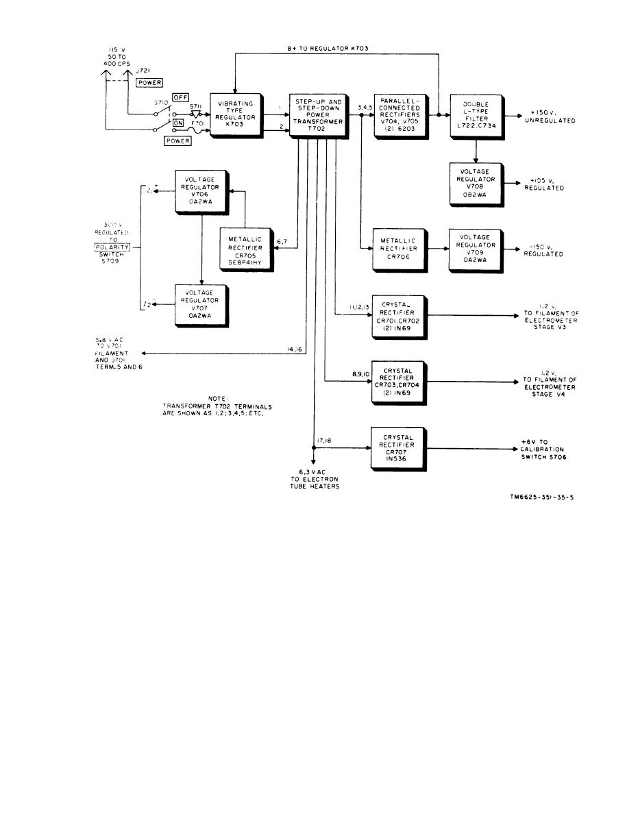 Figure 6. Power supply, block diagram.
the high-voltage center-tapped secondary
i d e n t i c a l pair of crystal rectifiers, CR703
w i n d i n g at terminals 3 and 5 of power
and CR704, which are connected to an addi-
t r a n s f o r m e r T702. The dc output of the
t i o n a l center-tapped secondary winding-
d i o d e is maintained at -150 volts with
( t e r m i n a l s 8, 9, and 10) of power trans-
respect to chassis ground by voltage reg-
f o r m e r T702.
ulator V709.
f. +6- Volt Power Circuit. Crystal diode
e. 1.2-Volt Power Circuits. T w o s e p a -
CR707 is connected to the 6.3-volt ac
rate outputs of 1.2-volts are provided for
secondary winding (terminals 17 and 18) of
electrometer stages V3 and V4. Oneoutput
power transformer T702. The rectified
is developed by the connection of crystal
6-volt dc output of this diode is used as
rectifiers CR701 and CR702 to the center-
energizing voltage for coaxial relays K701
t a p p e d secondary winding (terminals 11,
a n d K702, through the toggle action of
1 2 , and 13) of power transformer T702.
calibration switch S706.
T h e second output is developed by an
g. 300- Volt Power Circuit. A n o t h e r
15
|
|
Privacy Statement - Press Release - Copyright Information. - Contact Us |
