 |
|||
|
|
|||
|
Page Title:
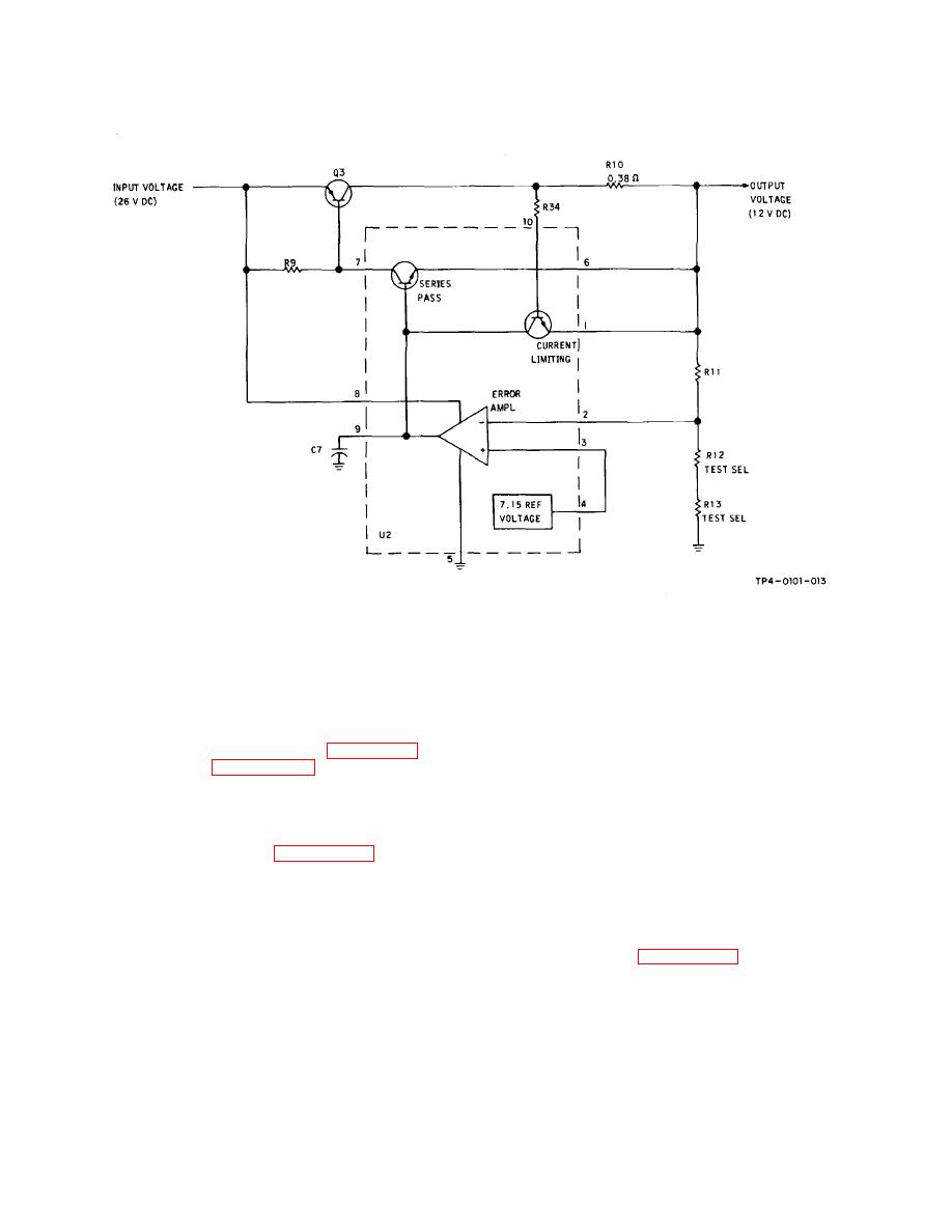
Figure 4-8. +12-V Series Regulator, Simplified Schematic Diagram |
|
||
| ||||||||||
|
|  TO 31R2-2GRC171-2
TM 11-5820-815-14
NAVELEX 0967-LP-544-5010
Figure 4-8. +12-V Series Regulator, Simplified Schematic Diagram
4-224. The rf filter is a tunable bandpass filter that
Resistor R30 is test selected to set the output voltage to
provides a high degree of selectivity between the
approximately +22 V dc. The output current from the 22-
antenna and power amplifier or antenna and receiver.
V series regulator is not current limited.
The rf filter module includes the rf filter, mechanical drive
train, and servo motor with position feedback
4-221. RF FILTER MODULE A7.
potentiometer, whereas d/a servo amplifier module A1
provides control to the servo motor to position the rf filter
4-222. Refer to the block diagram of figure FO-9 and
to the desired frequency.
schematic diagram of figure FO-24 while reading the
following circuit descriptions.
Unless otherwise
4-225. The directional coupler senses forward and
specified, reference designators apply to components of
reflected power into the antenna during transmit mode.
rf filter module A7.
Outputs from the directional coupler are amplified and
fed back to the power amplifier module A8 for automatic
4-223. GENERAL. Refer to figure FO-9. Rf filter
load control and to the meter circuit on the front panel of
module A7 contains a transmit/receive switch, rf filter,
chassis A10. Percent modulation, derived from the
and directional coupler. The transmit/receive switch
forward power output, is fed to the meter circuit.
consists of three pin diodes (transmit series diode,
receive series diode, and receive shunt diode) that
4-226. TRANSMIT/RECEIVE SWITCH AND CONTROL
together function as a transfer switch and receive signal
CIRCUIT. Refer to figure FO-24. Transmit series diode
attenuator. In transmit mode, the transmit series diode
CR1, receive series diode CR2, and receive shunt diode
provides minimum attenuation to the transmit rf signal
CR3 are pin-type diodes that exhibit the characteristic of
while the receive series and receive shunt diodes provide
providing an increasing rf resistance as the dc current
about 36 dB of isolation between the antenna and
through the diodes decreases. Maximum resistance is
receiver. In receive mode, the receive series and
attained when the diodes are reverse biased. Minimum
receive shunt diodes provide from 0- up to about 36-dB
resistance is attained when CR1 is forward biased at
attenuation for AGC control and receiver overload
about
100
protection. The transmit series diode provides about 20
dB of isolation between the antenna and power amplifier.
4-40
|
|
Privacy Statement - Press Release - Copyright Information. - Contact Us |
