 |
|||
|
|
|||
|
Page Title:
The CVDOW signal from module A3 |
|
||
| ||||||||||
|
|  TM 11-5820-695-35
highest rate group, ground at U15E cuts R40 and R42
signal at U11A-5 is inverted in U3 and applied to U14.
out of the circuit and the bias and gain of Q1 are lowest.
When CVDOW is logic 0, U13D-11 and U13C-8 provide
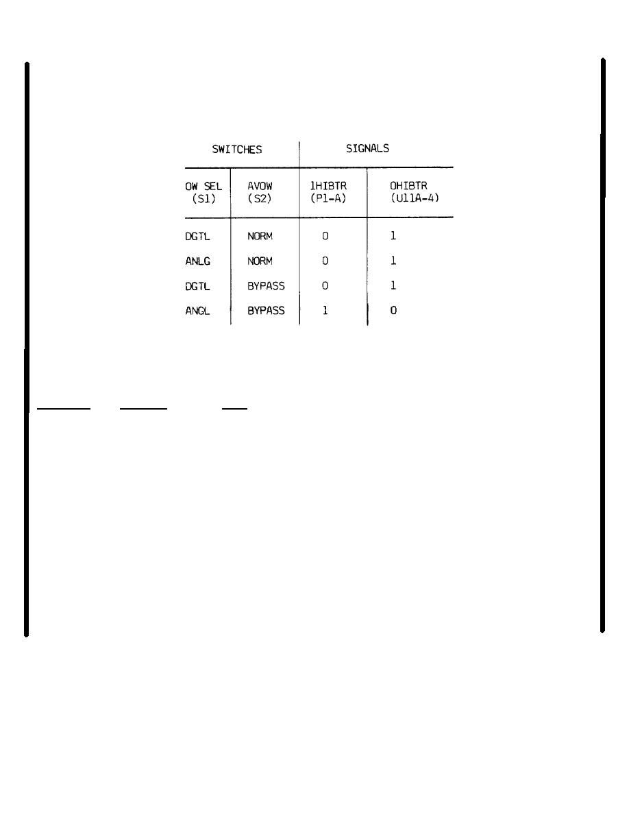
(6) The CVDOW signal from module A3
is applied to inverters U13C and U13D. It is gain-
a high impedance output, isolating U13D and U13C
from the bias network. The rate group
adjusted according to the data rate in use by U13C,
U13D, buffers and gain of Q1 are highest. For the
U15 and transistor Q1, under control of signals from
and therefore of the GACVDOW signal level at the
DATA RATE SEL (MB) switch S4, in three rate groups.
emitter of Q1. This signal level is given in the chart
The rate groups and the CVDOW signal levels are as
above. When CVDOW is logic 1, U13D-11 and U13C-8
follows:
are logic 0, Q1 is cut off and the GACVDOW signal is
logic 0. The GACVDOW signal is connected through a
Rate Group
Data Rate
3-pole Butterworth filter (R35/C5, L1, R33/C6) to the
Level
input of buffer amplifier U14. The data signal from
inverter U3 ((5) above) is also applied to U14. The two
A (P1-R)
9.36 or 18.72
2.2v
signals are linearly added in R44 which is used to adjust
B (P1-S)
2.048 to 4.9152
3.3v
the gain of U14 to unity.
The output of U14,
approximately 2 v peak-to-peak, is reduced to 1 v peak-
C (P1-P)
1.024 to 1.536
4.4v
to-peak in a T-network attenuator (R45, R46, R49) and
routed to the radio (P1-18 and -V).
U13 and U15 are open collector type IC's that is, a logic
1 output is a high impedance (open circuit) instead of a
(7) IC's U1, U2, U5, U6, U8 and U9
logic 1 level voltage. Logic 0 is applied to the U15
comprise the status monitoring circuits. U2A and B and
buffer corresponding to the rate group in which the
U9A and B are retriggerable monostables with a timed
operating data rate falls. Logic 1 is applied through pull
output of 150 msec. When the monitored input signal at
up resistors R37, R39 and R41.
The buffer
pin 2 or pin 9 is active and provides a logic 1 input at
corresponding to the selected rate has logic 0 output. It
least once every 150 msec, the monostable is
grounds the junction of R38/R40 (U15E) or R40/R42
maintained in the set state (Q at logic 1, Q at logic 0). If
(U15D) or it grounds R42 at U15F. These resistors with
the monitored signal fails, the monostable times out
CR2 and R35 determine the bias and therefore the gain
after 150 msec and is reset
of Q1 when it is turned on. For the lowest rate group
(U15F), all resistors are in the bias network and bias
signals (A, B, C) then determine the bias and gain of Q1
Change 6 2-16.12
|
|
Privacy Statement - Press Release - Copyright Information. - Contact Us |
