 |
|||
|
|
|||
|
|
|||
| ||||||||||
|
|  TM 11-5820-509-35
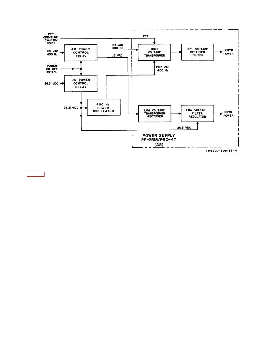
Figure 2-4. Power Supply Circuits, Block Diagram.
receiver mixer Q11 with the output of Q10. The
2-5. Receive Signal Path
difference between these two signals, approximately
500 kHz, is applied to follower Q9 and routed to the if.
a. In the receive mode, the 2.0to 11.999-MHz rf
amplifier circuits of amplifier-modulator A2.
After
signal from the antenna system is routed through the
amplification by A2Q2, the if. signal is routed through
normally-closed contacts of t/r relay K101 in the power
bandpass filter FL1 where the if. carrier signal and the
amplifier compartment to receiver antenna relay K5 on
undesired sideband are greatly attenuated. Following
the Main chassis of the receiver-transmitter. Both of
additional amplification by if. amplifiers Q3 through Q5,
these relays are deenergized in the receive mode, but
this signal is demodulated by the product detector
are energized by the voice-operated-transmit (vox)
circuit.
circuits during transmitter operation. The receive rf
signals from the normally closed contacts of receiver
c. The audio component of the if. signal is
signal data translator A3 and are amplified by rf
extracted by mixing the if. signal with a carrier injection
amplifiers V1 and V2. These stages are also used tc
signal (500-kHz standard) at the intermediate frequency.
amplify transmit rf signals when the transmit mode is
The output of the product detector is then passed
selected, and are tuned to the operating frequency
through a low-pass filter to remove undesired
selected by the frequency control knobs on the front
frequencies caused by mixing and then amplified by
panel of RT671/PRC-47. The additional selectivity
driver stage Q10 and audio output amplifier Q11WQ12X
provided by these tuned circuits restricts the signals
in audio frequency amplifier A1. This amplified audio
applied to the rf amplifier input to those that are on, or
signal is applied to the corrected audio output device
very near, the selected operating channel.
through front panel VOLUME control R11-R12. Once
b. Relay A3K1 is deenergized during receiver
the average audio output level has been established by
operation and its contacts route the amplified rf signal
the setting of the VOLUME control. automatic gain
from the second rf amplifier (V2) to follower Q1O.
control (agc) circuits in audio frequency amplifier A1
(During transmit periods. A3K 1 is energized and
maintain the output level relatively constant despite
capacitor C187 is connected to the output of V2.) The
fading signal conditions. The +agc voltage' from agc
hf oscillator signal from the frequency control circuits is
amplifier Q9 is applied to if. amplifiers Q2 and Q3 while
isolated by follower 24 Q12 and is then mixed in
the -agc output of detector CR12-CR13 is applied to
2-8
|
|
Privacy Statement - Press Release - Copyright Information. - Contact Us |
