 |
|||
|
|
|||
|
Page Title:
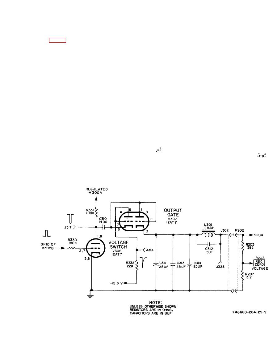
Figure 2-8. Voltage switch and output gate, simplified schematic diagram. |
|
||
| ||||||||||
|
|  TM 11-6660-204-25
b. Voltage switch tube V306 is normally held
affect the extent of discharge. When the control-
beyond cutoff by the high grid bias applied to tube
ling pulse is over, voltage switching tube V306 is
V305B through grid-current limiting resistor
a g a i n cut off and capacitor C310 recharges
R330 (fig. 2-7). When a positive pulse is devel-
through resistor R331, tube V307B, and the low
oped by the univibrator, the grid of tube V306 is
impedance filter and load network between the
driven rapidly from cutoff to zero or slightly posi-
cathode of tube V307B and ground. To assure an
tive, and the plate current of switch tube V306
equal amount of energy per pulse being stored in
rises steeply to a steady value. This value of plate
filter capacitors C311, C313, and C314, the values
current and its time of duration are essentially
of resistor R331 and capacitor C310 have been
the same for each pulse. Plate-1oad resistor R331
carefully designed to avoid the variations of re-
is a precision wire-wound type and, therefore, be-
sistance and capacitance that normally occur as a
cause the plate current is essentially the same for
result of changes in temperature and/or humid-
each pulse, the voltage drop produced across resis-
ity; other resistors and capacitors will not be sub-
tor R331 is also essentially the same throughout
stituted for these two particular items. The charg-
each pulse.
ing time for capacitor C310 is normally between
one-fifth and one-tenth of the period of the high-
c. Under static conditions of tube V306, capaci-
est pulse recurrence frequency that will be en-
tor C310 is charged to 300 volts. When a positive
countered, so there is always sufficient time for
pulse is applied to the grid of tube V306, the re-
the capacitor to recover its full charge between
sulting plate-cathode conductively serves as a
pulses.
closed circuit to permit a discharging current to
occur. The low resistance of the tube drops the
d. Because of the high value of capacity in the
plate potential steeply to about 25 volts. The dis-
parallel combination of C311, C313, and C314 (75
charge path on the negative side of capacitor
total), only a few microvolt of charge are
C310 may be traced through tube V307A and re-
built up on each pulse. Choke L301 and its
sistor R332. The time constant of this circuit is
shunt capacitor C312 resonate at approximately
relatively low, so the discharge is completed long
10 CPS, which increases the series filtering effect
before the end of the controlling pulse; thus small
at the low end of the af signal frequency scale. At
variations in pulse duration cannot appreciably
the high end, further filtering is accomplished at
|
|
Privacy Statement - Press Release - Copyright Information. - Contact Us |
