 |
|||
|
|
|||
|
Page Title:
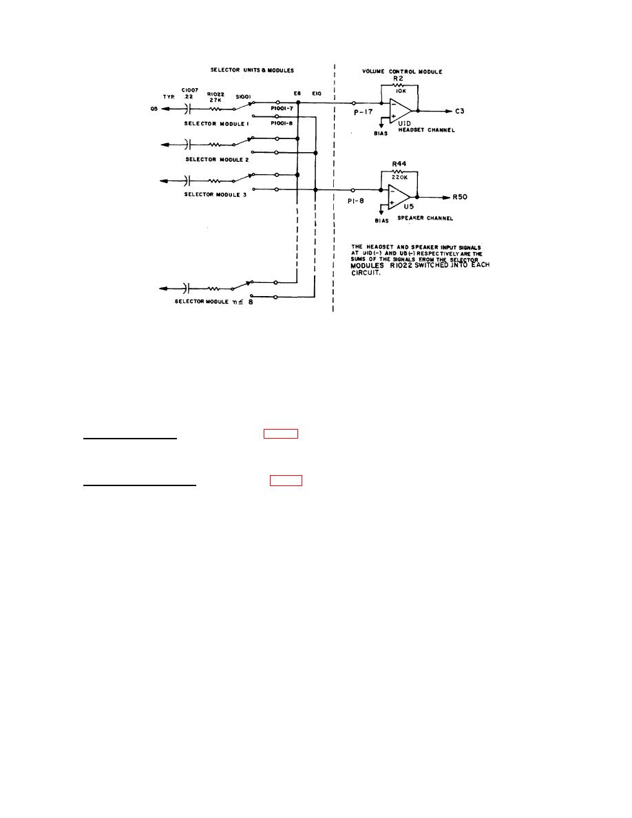
Figure 2-10. Summing Circuits in Speaker & Headset Amplifier Inputs |
|
||
| ||||||||||
|
|  TM 11-5895-1141-34
Figure 2-10. Summing Circuits in Speaker & Headset Amplifier Inputs
high frequencies. The output of operational amplifier U5 is then coupled via SPEAKER VOLUME control resistor R50,
which provides for a 20 dB signal reduction when fully counterclockwise. Signals picked off the arm of resistor R50 are fed
via capacitor C25 to pin 12 of connector P1 for input to the speaker amplifier board assembly. Resistor R47 is part of the
input biasing network. The SPEAKER VOLUME control also supplies current through a second input resistor R32 to the
summing point of operational amplifier U1A whose output, representing the sum of loudspeaker and headset signals, is
fed via resistor R35 and pin 17, to the recorder circuits, if used.
(3) Regulated Amplifier. Refer to figure FO-10. The volume control module contains a regulated amplifier
consisting of U2, U4, Q1, R3 and associated components. This amplifier is identical in performance to the regulated
amplifier previously described in the paragraph on the microphone amplifier/lamp brightener module in this section.
(4) Headset Driver Amplifier. Refer to figure FO-10. The regulated signal at the output of operational amplifier U3
is fed to an
2-24
|
|
Privacy Statement - Press Release - Copyright Information. - Contact Us |
