 |
|||
|
|
|||
|
Page Title:
The operating frequency of oscillator U18 |
|
||
| ||||||||||
|
|  TM 11-5820-695-35
control voltage from the output of the phase lock at U4-
(4) Data rate select logic circuits U2, U6, U7,
10 is applied to CR5 through an isolating and filtering
UO1 and U11 under control of signals from DATA RATE
network (CR8, CR9, C26, R25, R28, L12). Zener diodes
SEL (MB) switch lA12S4 provide the two required rate
CR8 and CR9 limit the range of this voltage to protect
select functions. Gates U2, U7, and U11 provide the
varactor diode CR5. A bias voltage, applied at the
crystal select function. Gates U6 and U10 provide for
cathode of CR5, sets its operating (pull-in) range. This
division of the oscillator signal by the factor required to
voltage is derived from +12 vdc through R27, CR7 and
produce the selected data rate clock. Dual sinewave
filter capacitor C27. It is applied to CR5 through an
outputs at U18-2 and -3 are coupled through C4/R15
isolating and filtering network (CR6, C25, R24, R26, and
and C5/R16 to squarewave generator U19. The inputs
L11).
at U19-4 and -5 balanced to ground by R12/R13. Dual
complementary squarewave outputs at U19-13 and -4
(3) The operating frequency of oscillator U18
are applied to the divider circuits and to clock gate U14.
is determined by the crystal selected. The output signal
of U18 must be divided by some factor to provide the
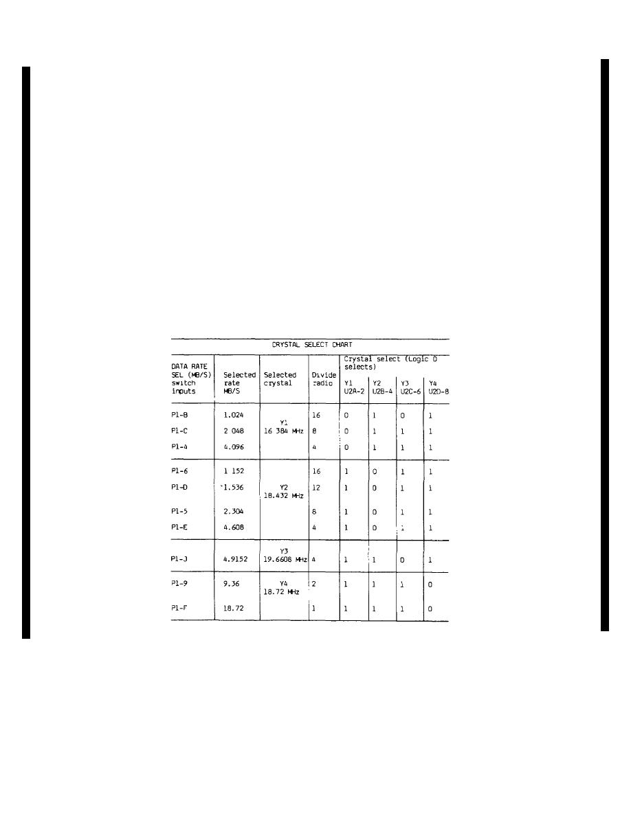
(5) Crystal Y1 is used for three data rates, Y2
clock signal at the operating data rate. This is required
for four data rates, Y3 for one data rate and Y4 for two
because the crystal frequency is higher than the data
data rates. The input signals from DATA RATE SEL
rate and because crystals Y1, Y2, and Y4 are used for
(MB) switch lA12S4 at the pins listed in the crystal select
more than one data rate. These functions are discussed
chart below are connected to the rate select logic gates.
in (4) through (6) below. The clock signal must be
Each of these input signals is logic I (high), except the
synchronized to the timing of the data signal. This
input corresponding to the selected rate. This signal is
function is discussed in (8) and (9) below.
logic 0 (low). The input lines have pull-up resistors (U8)
which
Change 6 2-24.4
|
|
Privacy Statement - Press Release - Copyright Information. - Contact Us |
