 |
|||
|
|
|||
|
|
|||
| ||||||||||
|
|  TM 11-5820-695-35
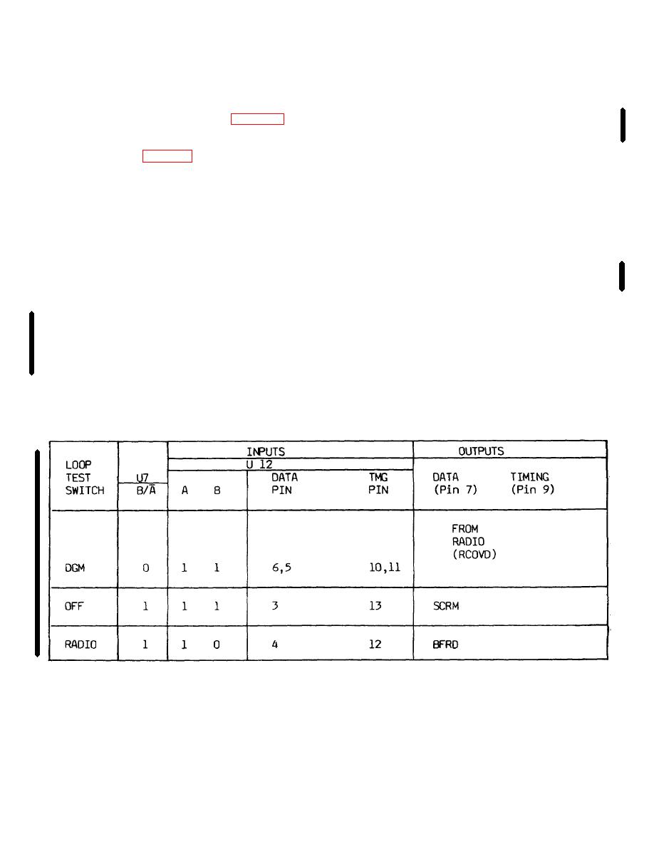
switch (53). Multiplexer U12 connects one of the three
(3) below). Thus multiplexer U7 acts as the cable
pairs of input signals to outputs 1Y (pin 7) and 2Y (pin 9)
loopback switch. In normal operation, the DSCRM
according to the logic states of signals A and B. The
DATA and TIMING signals from the remote site are
three possible combinations of logic states for signals
passed by U7 and routed to the DGM (fig. 5-8.2, solid
B/A (U7), A and B are listed in the chart below along
lines in U7). In cable loopback mode, the DATA IN and
with the corresponding positions of the LOOP TEST
TMG IN signals from the DGM are passed by U7 and
switch in column 1. Columns 4, 5 and 6 indicate which
returned to the DGM (fig. 5-8.2, dashed lines in U7).
input pins are connected to output pins 7 and 9 and the
signals passed by U12 for each logic state of signals A
(3) The DATA output at U7-4 is retimed
and B. Thus U12 functions as the radio loopback
in U11 and converted to a balanced signal in line driver
switch: it selects the signal to be sent to the radio
U10. The timing signal from U7-7, twice inverted in
transmitter ((5) below) under control of the LOOP TEST
U6B and U6A, is similarly converted in U10. U6A and
switch.
U6B are used to provide a time delay to compensate for
the delay the data signal encounters in passing through
(5) The data output signal at U12-7 is
U11B. Resistors R17, R18, R19, R21, R22 with C4 and
applied to U11A-2. U11A is operational as long as the
signal at reset input pin 4 is logic 1. When this signal is
network.
logic 0, U11A is locked in reset and the data signal from
U12 is blocked. Signal 1HIBTR (P1-A) is controlled by
(4) Three pairs of input signals are
OW SEL switch S1 and AVOW switch S2. Signal
applied to multiplexer U12: 1) RCOVD DATA at pins 5
1HIBTR is inverted in U6F and applied at U11A-4 as
and 6 from module A5 and TIMING at pins 10 and 11
signal 0HIBTR.
The switch positions and the
from DSCRM or BFRD TMG; 2) BFRD DATA and
corresponding logic state of the signal at U11A-4 are
TIMING at pins 4 and 12, from U4; 3) SCRM DATA and
given in the chart on the following page. As indicated in
TMG at pins 3 and 13 from module A3. Multiplexer U12
the chart, the signal at U11-4 is logic 0 only when the
is a dual 4-pole electronic switch; switching operation is
switches select the analog orderwire bypass mode. For
controlled by signals at pins 14 (A) and 2 (B). The A
other switch positions U11A is operational. The data
(pin 14) logic 1 level signal is supplied by pull-up resistor
signal from U12 is retimed in U11A. The output
R56. The B (pin 2) signal is supplied by LOOP TEST
Change 6 2-16.11
|
|
Privacy Statement - Press Release - Copyright Information. - Contact Us |
